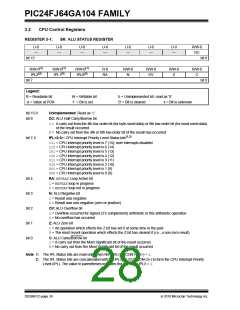
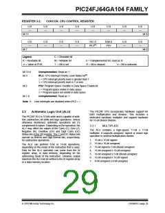
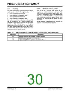
PIC24FJ64GA104 FAMILY
4.1.1
PROGRAM MEMORY
ORGANIZATION
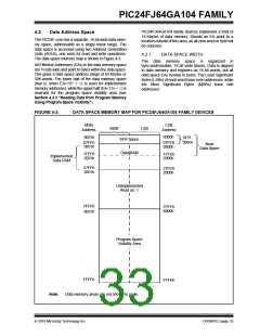
4.1.3
FLASH CONFIGURATION WORDS
In PIC24FJ64GA104 family devices, the top four words
of on-chip program memory are reserved for configura-
tion information. On device Reset, the configuration
information is copied into the appropriate Configuration
registers. The addresses of the Flash Configuration
Word for devices in the PIC24FJ64GA104 family are
shown in Table 4-1. Their location in the memory map
is shown with the other memory vectors in Figure 4-1.
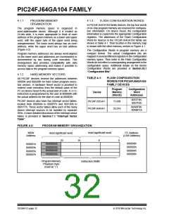
The program memory space is organized in
word-addressable blocks. Although it is treated as
24 bits wide, it is more appropriate to think of each
address of the program memory as a lower and upper
word, with the upper byte of the upper word being
unimplemented. The lower word always has an even
address, while the upper word has an odd address
(Figure 4-2).
The Configuration Words in program memory are a
compact format. The actual Configuration bits are
mapped in several different registers in the configuration
memory space. Their order in the Flash Configuration
Words do not reflect a corresponding arrangement in the
configuration space. Additional details on the device
Configuration Words are provided in Section 25.1
“Configuration Bits”.
Program memory addresses are always word-aligned
on the lower word and addresses are incremented or
decremented by two during code execution. This
arrangement also provides compatibility with data
memory space addressing and makes it possible to
access data in the program memory space.
4.1.2
HARD MEMORY VECTORS
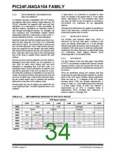
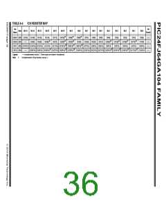
TABLE 4-1:
FLASH CONFIGURATION
WORDS FOR PIC24FJ64GA104
FAMILY DEVICES
All PIC24F devices reserve the addresses between
00000h and 000200h for hard coded program execu-
tion vectors. A hardware Reset vector is provided to
redirect code execution from the default value of the
PC on device Reset to the actual start of code. A GOTO
instruction is programmed by the user at 000000h with
the actual address for the start of code at 000002h.
Program
Memory
(Words)
Configuration
Word
Addresses
Device
0057F8h:
0057FEh
PIC24F devices also have two interrupt vector tables,
located from 000004h to 0000FFh and 000100h to
0001FFh. These vector tables allow each of the many
device interrupt sources to be handled by separate
ISRs. A more detailed discussion of the interrupt vector
tables is provided in Section 7.1 “Interrupt Vector
Table”.
PIC24FJ32GA1
PIC24FJ64GA1
11,008
22,016
00ABF8h:
00ABFEh
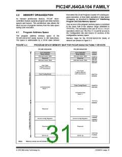
FIGURE 4-2:
PROGRAM MEMORY ORGANIZATION
least significant word
8
MSW
Address
PC Address
(LSW Address)
most significant word
23
16
0
000000h
000002h
000004h
000006h
00000000
000001h
000003h
000005h
000007h
00000000
00000000
00000000
Program Memory
‘Phantom’ Byte
(read as ‘0’)
Instruction Width
DS39951C-page 32
2010 Microchip Technology Inc.

 MICROCHIP [ MICROCHIP ]