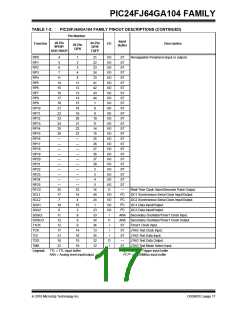
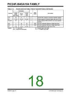
PIC24FJ64GA104 FAMILY
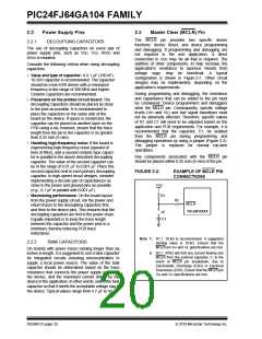
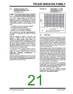
FIGURE 2-3:
FREQUENCY vs. ESR
PERFORMANCE FOR
SUGGESTED VCAP
2.4
Voltage Regulator Pins
(ENVREG/DISVREG and
VCAP/VDDCORE)
10
1
Note:
This section applies only to PIC24FJ
devices with an on-chip voltage regulator.
The on-chip voltage regulator enable/disable pin
(ENVREG or DISVREG, depending on the device
family) must always be connected directly to either a
supply voltage or to ground. The particular connection
is determined by whether or not the regulator is to be
used:
0.1
0.01
• For ENVREG, tie to VDD to enable the regulator,
or to ground to disable the regulator
0.001
0.01
0.1
1
10
100
1000 10,000
Frequency (MHz)
• For DISVREG, tie to ground to enable the
regulator or to VDD to disable the regulator
Note:
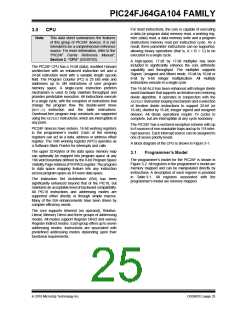
Data for Murata GRM21BF50J106ZE01 shown.
Measurements at 25°C, 0V DC bias.
Refer to Section 25.2 “On-Chip Voltage Regulator”
for details on connecting and using the on-chip
regulator.
2.5
ICSP Pins
When the regulator is enabled, a low-ESR (<5Ω)
capacitor is required on the VCAP/VDDCORE pin to
stabilize the voltage regulator output voltage. The
VCAP/VDDCORE pin must not be connected to VDD, and
must use a capacitor of 10 F connected to ground. The
type can be ceramic or tantalum. A suitable example is
the Murata GRM21BF50J106ZE01 (10 F, 6.3V) or
equivalent. Designers may use Figure 2-3 to evaluate
ESR equivalence of candidate devices.
The PGECx and PGEDx pins are used for In-Circuit
Serial Programming (ICSP) and debugging purposes.
It is recommended to keep the trace length between
the ICSP connector and the ICSP pins on the device as
short as possible. If the ICSP connector is expected to
experience an ESD event, a series resistor is recom-
mended, with the value in the range of a few tens of
ohms, not to exceed 100Ω.
Pull-up resistors, series diodes and capacitors on the
PGECx and PGEDx pins are not recommended as they
will interfere with the programmer/debugger communi-
cations to the device. If such discrete components are
an application requirement, they should be removed
from the circuit during programming and debugging.
Alternatively, refer to the AC/DC characteristics and
timing requirements information in the respective
device Flash programming specification for information
on capacitive loading limits and pin input voltage high
(VIH) and input low (VIL) requirements.
The placement of this capacitor should be close to
VCAP/VDDCORE. It is recommended that the trace
length not exceed 0.25 inch (6 mm). Refer to
Section 28.0 “Electrical Characteristics” for
additional information.
When the regulator is disabled, the VCAP/VDDCORE pin
must be tied to a voltage supply at the VDDCORE level.
Refer to Section 28.0 “Electrical Characteristics” for
information on VDD and VDDCORE.
For device emulation, ensure that the “Communication
Channel Select” (i.e., PGECx/PGEDx pins) programmed
into the device matches the physical connections for the
ICSP to the Microchip debugger/emulator tool.
For more information on available Microchip
development tools connection requirements, refer to
Section 26.0 “Development Support”.
2010 Microchip Technology Inc.
DS39951C-page 21

 MICROCHIP [ MICROCHIP ]