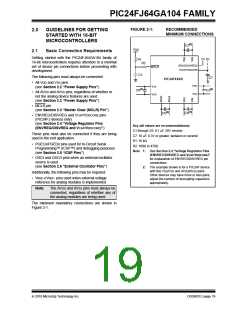
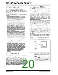
PIC24FJ64GA104 FAMILY
If your application needs to use certain A/D pins as
analog input pins during the debug session, the user
application must modify the appropriate bits during
initialization of the ADC module, as follows:
2.7
Configuration of Analog and
Digital Pins During ICSP
Operations
If an ICSP compliant emulator is selected as a debug-
ger, it automatically initializes all of the A/D input pins
(ANx) as “digital” pins. Depending on the particular
device, this is done by setting all bits in the ADnPCFG
register(s), or clearing all bit in the ANSx registers.
• For devices with an ADnPCFG register, clear the
bits corresponding to the pin(s) to be configured
as analog. Do not change any other bits, particu-
larly those corresponding to the PGECx/PGEDx
pair, at any time.
All PIC24F devices will have either one or more
ADnPCFG registers or several ANSx registers (one for
each port); no device will have both. Refer to
Section 21.0 “10-Bit High-Speed A/D Converter”)
for more specific information.
• For devices with ANSx registers, set the bits
corresponding to the pin(s) to be configured as
analog. Do not change any other bits, particularly
those corresponding to the PGECx/PGEDx pair,
at any time.
The bits in these registers that correspond to the A/D
pins that initialized the emulator must not be changed
by the user application firmware; otherwise,
communication errors will result between the debugger
and the device.
When a Microchip debugger/emulator is used as a
programmer, the user application firmware must
correctly configure the ADnPCFG or ANSx registers.
Automatic initialization of this register is only done
during debugger operation. Failure to correctly
configure the register(s) will result in all A/D pins being
recognized as analog input pins, resulting in the port
value being read as a logic '0', which may affect user
application functionality.
2.8
Unused I/Os
Unused I/O pins should be configured as outputs and
driven to a logic low state. Alternatively, connect a 1 kΩ
to 10 kΩ resistor to VSS on unused pins and drive the
output to logic low.
2010 Microchip Technology Inc.
DS39951C-page 23

 MICROCHIP [ MICROCHIP ]