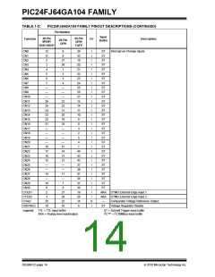
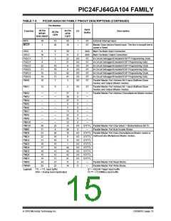
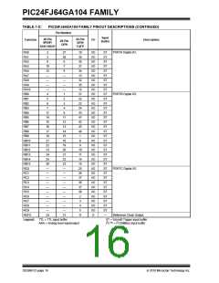
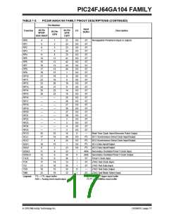
PIC24FJ64GA104 FAMILY
TABLE 1-2:
PIC24FJ64GA104 FAMILY PINOUT DESCRIPTIONS (CONTINUED)
Pin Number
Input
Buffer
28-Pin
SPDIP/
SOIC/SSOP
44-Pin
QFN/
TQFP
Function
I/O
Description
28-Pin
QFN
VCAP
20
13, 28
20
17
10, 25
17
7
28, 40
7
P
P
P
—
—
—
External Filter Capacitor Connection (regulator enabled).
Positive Supply for Peripheral Digital Logic and I/O Pins.
VDD
VDDCORE
Positive Supply for Microcontroller Core Logic (regulator
disabled).
VREF-
VREF+
VSS
3
2
28
27
20
19
I
I
ANA
ANA
—
A/D and Comparator Reference Voltage (low) Input.
A/D and Comparator Reference Voltage (high) Input.
Ground Reference for Logic and I/O Pins.
8, 27
5, 24
29, 39
P
Legend:
TTL = TTL input buffer
ANA = Analog level input/output
ST = Schmitt Trigger input buffer
I C™ = I C/SMBus input buffer
2
2
DS39951C-page 18
2010 Microchip Technology Inc.

 MICROCHIP [ MICROCHIP ]