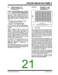
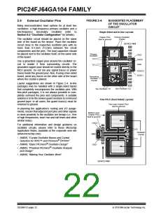
PIC24FJ64GA104 FAMILY
For most instructions, the core is capable of executing
a data (or program data) memory read, a working reg-
3.0
CPU
Note:
This data sheet summarizes the features
of this group of PIC24F devices. It is not
intended to be a comprehensive reference
source. For more information, refer to the
“PIC24F Family Reference Manual”,
Section 2. “CPU” (DS39703).
ister (data) read, a data memory write and a program
(instruction) memory read per instruction cycle. As a
result, three parameter instructions can be supported,
allowing trinary operations (that is, A + B = C) to be
executed in a single cycle.
A high-speed, 17-bit by 17-bit multiplier has been
included to significantly enhance the core arithmetic
capability and throughput. The multiplier supports
Signed, Unsigned and Mixed mode, 16-bit by 16-bit or
8-bit by 8-bit integer multiplication. All multiply
instructions execute in a single cycle.
The PIC24F CPU has a 16-bit (data), modified Harvard
architecture with an enhanced instruction set and a
24-bit instruction word with a variable length opcode
field. The Program Counter (PC) is 23 bits wide and
addresses up to 4M instructions of user program
memory space. A single-cycle instruction prefetch
mechanism is used to help maintain throughput and
provides predictable execution. All instructions execute
in a single cycle, with the exception of instructions that
change the program flow, the double-word move
(MOV.D) instruction and the table instructions.
Overhead-free program loop constructs are supported
using the REPEATinstructions, which are interruptible at
any point.
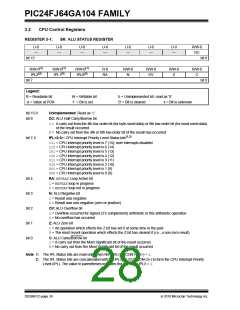
The 16-bit ALU has been enhanced with integer divide
assist hardware that supports an iterative non-restoring
divide algorithm. It operates in conjunction with the
REPEATinstruction looping mechanism and a selection
of iterative divide instructions to support 32-bit (or
16-bit), divided by 16-bit, integer signed and unsigned
division. All divide operations require 19 cycles to
complete, but are interruptible at any cycle boundary.
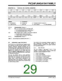
The PIC24F has a vectored exception scheme with up
to 8 sources of non-maskable traps and up to 118 inter-
rupt sources. Each interrupt source can be assigned to
one of seven priority levels.
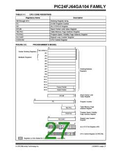
PIC24F devices have sixteen, 16-bit working registers
in the programmer’s model. Each of the working
registers can act as a data, address or address offset
register. The 16th working register (W15) operates as
a Software Stack Pointer for interrupts and calls.
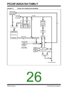
A block diagram of the CPU is shown in Figure 3-1.
The upper 32 Kbytes of the data space memory map
can optionally be mapped into program space at any
16K word boundary defined by the 8-bit Program Space
Visibility Page Address (PSVPAG) register. The program
to data space mapping feature lets any instruction
access program space as if it were data space.
3.1
Programmer’s Model
The programmer’s model for the PIC24F is shown in
Figure 3-2. All registers in the programmer’s model are
memory mapped and can be manipulated directly by
instructions. A description of each register is provided
in Table 3-1. All registers associated with the
programmer’s model are memory mapped.
The Instruction Set Architecture (ISA) has been
significantly enhanced beyond that of the PIC18, but
maintains an acceptable level of backward compatibility.
All PIC18 instructions and addressing modes are
supported either directly or through simple macros.
Many of the ISA enhancements have been driven by
compiler efficiency needs.
The core supports Inherent (no operand), Relative,
Literal, Memory Direct and three groups of addressing
modes. All modes support Register Direct and various
Register Indirect modes. Each group offers up to seven
addressing modes. Instructions are associated with
predefined addressing modes depending upon their
functional requirements.
2010 Microchip Technology Inc.
DS39951C-page 25

 MICROCHIP [ MICROCHIP ]