PIC24FJ64GA104 FAMILY
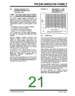
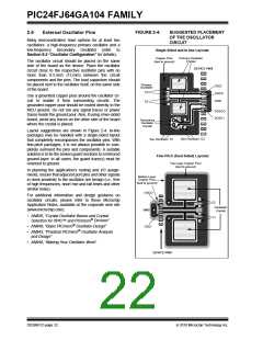
FIGURE 2-4:
SUGGESTED PLACEMENT
OF THE OSCILLATOR
CIRCUIT
2.6
External Oscillator Pins
Many microcontrollers have options for at least two
oscillators: a high-frequency primary oscillator and a
low-frequency Secondary Oscillator (refer to
Section 8.0 “Oscillator Configuration” for details).
Single-Sided and In-line Layouts:
Copper Pour
(tied to ground)
Primary Oscillator
Crystal
The oscillator circuit should be placed on the same
side of the board as the device. Place the oscillator
circuit close to the respective oscillator pins with no
more than 0.5 inch (12 mm) between the circuit
components and the pins. The load capacitors should
be placed next to the oscillator itself, on the same side
of the board.
DEVICE PINS
Primary
OSCI
OSCO
GND
Oscillator
C1
C2
`
`
Use a grounded copper pour around the oscillator cir-
cuit to isolate it from surrounding circuits. The
grounded copper pour should be routed directly to the
MCU ground. Do not run any signal traces or power
traces inside the ground pour. Also, if using a two-sided
board, avoid any traces on the other side of the board
where the crystal is placed.
SOSCO
SOSC I
Secondary
Oscillator
Crystal
`
Layout suggestions are shown in Figure 2-4. In-line
packages may be handled with a single-sided layout
that completely encompasses the oscillator pins. With
fine-pitch packages, it is not always possible to com-
pletely surround the pins and components. A suitable
solution is to tie the broken guard sections to a mirrored
ground layer. In all cases, the guard trace(s) must be
returned to ground.
Sec Oscillator: C2
Sec Oscillator: C1
Fine-Pitch (Dual-Sided) Layouts:
Top Layer Copper Pour
(tied to ground)
In planning the application’s routing and I/O assign-
ments, ensure that adjacent port pins and other signals
in close proximity to the oscillator are benign (i.e., free
of high frequencies, short rise and fall times and other
similar noise).
Bottom Layer
Copper Pour
(tied to ground)
OSCO
For additional information and design guidance on
oscillator circuits, please refer to these Microchip
Application Notes, available at the corporate web site
(www.microchip.com):
C2
Oscillator
Crystal
GND
• AN826, “Crystal Oscillator Basics and Crystal
Selection for rfPIC™ and PICmicro® Devices”
C1
• AN849, “Basic PICmicro® Oscillator Design”
OSCI
• AN943, “Practical PICmicro® Oscillator Analysis
and Design”
• AN949, “Making Your Oscillator Work”
DEVICE PINS
DS39951C-page 22
2010 Microchip Technology Inc.

 MICROCHIP [ MICROCHIP ]