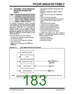
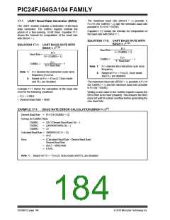
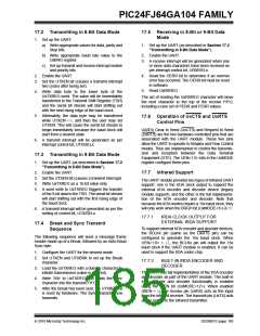
PIC24FJ64GA104 FAMILY
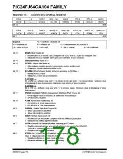
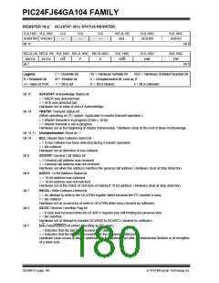
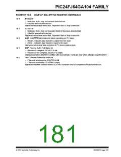
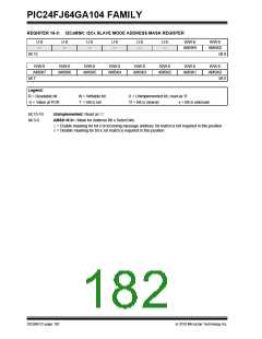
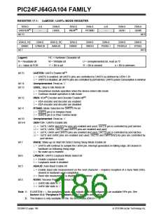
REGISTER 16-3: I2CxMSK: I2Cx SLAVE MODE ADDRESS MASK REGISTER
U-0
—
U-0
—
U-0
—
U-0
—
U-0
—
U-0
—
R/W-0
R/W-0
AMSK9
AMSK8
bit 15
bit 8
R/W-0
R/W-0
R/W-0
R/W-0
R/W-0
R/W-0
R/W-0
R/W-0
AMSK7
AMSK6
AMSK5
AMSK4
AMSK3
AMSK2
AMSK1
AMSK0
bit 7
bit 0
Legend:
R = Readable bit
W = Writable bit
‘1’ = Bit is set
U = Unimplemented bit, read as ‘0’
‘0’ = Bit is cleared x = Bit is unknown
-n = Value at POR
bit 15-10
bit 9-0
Unimplemented: Read as ‘0’
AMSK<9:0>: Mask for Address Bit x Select bits
1= Enable masking for bit x of incoming message address; bit match is not required in this position
0= Disable masking for bit x; bit match is required in this position
DS39951C-page 182
2010 Microchip Technology Inc.

 MICROCHIP [ MICROCHIP ]