PIC24FJ64GA104 FAMILY
13.1 General Operating Modes
13.0 INPUT CAPTURE WITH
DEDICATED TIMERS
13.1.1
SYNCHRONOUS AND TRIGGER
MODES
Note:
This data sheet summarizes the features
of this group of PIC24F devices. It is not
intended to be a comprehensive reference
source. For more information, refer to the
“PIC24F Family Reference Manual”,
Section 34. “Input Capture with
Dedicated Timer” (DS39722).
By default, the input capture module operates in a
free-running mode. The internal 16-bit counter ICxTMR
counts up continuously, wrapping around from FFFFh
to 0000h on each overflow, with its period synchronized
to the selected external clock source. When a capture
event occurs, the current 16-bit value of the internal
counter is written to the FIFO buffer.
Devices in the PIC24FJ64GA104 family all feature 5
independent input capture modules. Each of the
modules offers a wide range of configuration and
operating options for capturing external pulse events
and generating interrupts.
In Synchronous mode, the module begins capturing
events on the ICx pin as soon as its selected clock
source is enabled. Whenever an event occurs on the
selected sync source, the internal counter is reset. In
Trigger mode, the module waits for a Sync event from
another internal module to occur before allowing the
internal counter to run.
Key features of the input capture module include:
• Hardware-configurable for 32-bit operation in all
modes by cascading two adjacent modules
Standard, free-running operation is selected by setting
the SYNCSEL bits to ‘00000’ and clearing the ICTRIG
bit (ICxCON2<7>). Synchronous and Trigger modes
are selected any time the SYNCSEL bits are set to any
value except ‘00000’. The ICTRIG bit selects either
Synchronous or Trigger mode; setting the bit selects
Trigger mode operation. In both modes, the SYNCSEL
bits determine the sync/trigger source.
• Synchronous and Trigger modes of output
compare operation, with up to 20 user-selectable
trigger/sync sources available
• A 4-level FIFO buffer for capturing and holding
timer values for several events
• Configurable interrupt generation
• Up to 6 clock sources available for each module,
driving a separate internal 16-bit counter
When the SYNCSEL bits are set to ‘00000’ and
ICTRIG is set, the module operates in Software Trigger
mode. In this case, capture operations are started by
manually setting the TRIGSTAT bit (ICxCON2<6>).
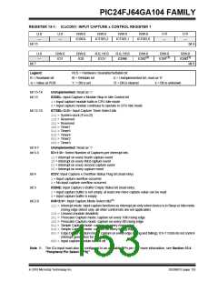
The module is controlled through two registers: ICxCON1
(Register 13-1) and ICxCON2 (Register 13-2). A general
block diagram of the module is shown in Figure 13-1.
FIGURE 13-1:
INPUT CAPTURE BLOCK DIAGRAM
ICM<2:0>
ICI<1:0>
Set ICxIF
Event and
Interrupt
Logic
Prescaler
Counter
1:1/4/16
Edge Detect Logic
and
Clock Synchronizer
(1)
ICx Pin
ICTSEL<2:0>
Increment
Clock
16
IC Clock
Sources
Select
ICxTMR
4-Level FIFO Buffer
16
Trigger and
Sync Logic
16
Reset
Trigger and
Sync Sources
ICxBUF
SYNCSEL<4:0>
Trigger
System Bus
ICOV, ICBNE
Note 1: The ICx inputs must be assigned to an available RPn pin before use. Please see Section 10.4 “Peripheral
Pin Select (PPS)” for more information.
2010 Microchip Technology Inc.
DS39951C-page 151

 MICROCHIP [ MICROCHIP ]