PIC24FJ64GA104 FAMILY
For 32-bit cascaded operations, the setup procedure is
slightly different:
13.1.2
CASCADED (32-BIT) MODE
By default, each module operates independently with
its own 16-bit timer. To increase resolution, adjacent
even and odd modules can be configured to function as
a single 32-bit module. (For example, modules 1 and 2
are paired, as are modules 3 and 4, and so on.) The
odd-numbered module (ICx) provides the Least Signif-
icant 16 bits of the 32-bit register pairs, and the even
module (ICy) provides the Most Significant 16 bits.
Wrap-arounds of the ICx registers cause an increment
of their corresponding ICy registers.
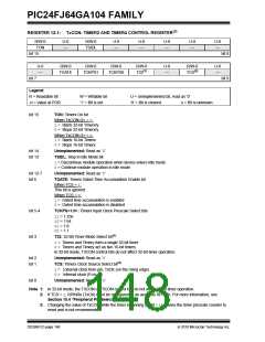
1. Set the IC32 bits for both modules
(ICyCON2<8> and (ICxCON2<8>), enabling the
even-numbered module first. This ensures the
modules will start functioning in unison.
2. Set the ICTSEL and SYNCSEL bits for both
modules to select the same sync/trigger and
time base source. Set the even module first,
then the odd module. Both modules must use
the same ICTSEL and SYNCSEL settings.
3. Clear the ICTRIG bit of the even module
(ICyCON2<7>); this forces the module to run in
Synchronous mode with the odd module,
regardless of its trigger setting.
Cascaded operation is configured in hardware by
setting the IC32 bits (ICxCON2<8>) for both modules.
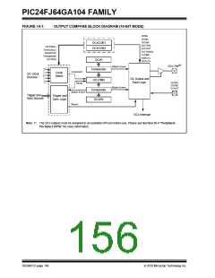
13.2 Capture Operations
4. Use the odd module’s ICI bits (ICxCON1<6:5>)
to the desired interrupt frequency.
The input capture module can be configured to capture
timer values and generate interrupts on rising edges on
ICx, or all transitions on ICx. Captures can be configured
to occur on all rising edges or just some (every 4th or
16th). Interrupts can be independently configured to
generate on each event or a subset of events.
5. Use the ICTRIG bit of the odd module
(ICxCON2<7>) to configure Trigger or
Synchronous mode operation.
Note:
For Synchronous mode operation, enable
the sync source as the last step. Both
input capture modules are held in Reset
until the sync source is enabled.
To set up the module for capture operations:
1. Configure the ICx input for one of the available
Peripheral Pin Select pins.
6. Use the ICM bits of the odd module
(ICxCON1<2:0>) to set the desired capture
mode.
2. If Synchronous mode is to be used, disable the
sync source before proceeding.
3. Make sure that any previous data has been
removed from the FIFO by reading ICxBUF until
the ICBNE bit (ICxCON1<3>) is cleared.
The module is ready to capture events when the time
base and the trigger/sync source are enabled. When
the ICBNE bit (ICxCON1<3>) becomes set, at least
one capture value is available in the FIFO. Read input
capture values from the FIFO until the ICBNE clears to
‘0’.
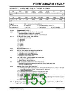
4. Set the SYNCSEL bits (ICxCON2<4:0>) to the
desired sync/trigger source.
5. Set the ICTSEL bits (ICxCON1<12:10>) for the
desired clock source. If the desired clock source
is running, set the ICTSEL bits before the Input
Capture module is enabled for proper
synchronization with the desired clock source.
For 32-bit operation, read both the ICxBUF and
ICyBUF for the full 32-bit timer value (ICxBUF for the
lsw, ICyBUF for the msw). At least one capture value is
available in the FIFO buffer when the odd module’s
ICBNE bit (ICxCON1<3>) becomes set. Continue to
read the buffer registers until ICBNE is cleared
(perform automatically by hardware).
6. Set the ICI bits (ICxCON1<6:5>) to the desired
interrupt frequency.
7. Select Synchronous or Trigger mode operation:
a) Check that the SYNCSEL bits are not set to
‘00000’.
b) For Synchronous mode, clear the ICTRIG
bit (ICxCON2<7>).
c) For Trigger mode, set ICTRIG and clear the
TRIGSTAT bit (ICxCON2<6>).
8. Set the ICM bits (ICxCON1<2:0>) to the desired
operational mode.
9. Enable the selected trigger/sync source.
DS39951C-page 152
2010 Microchip Technology Inc.

 MICROCHIP [ MICROCHIP ]