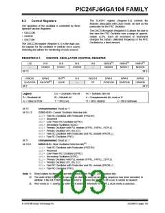
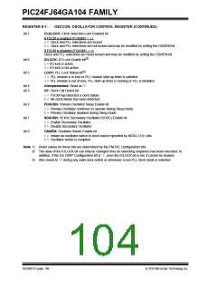
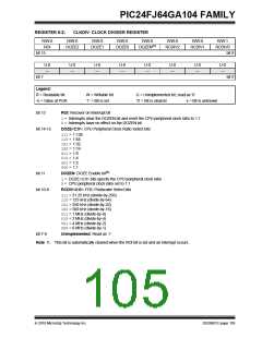
PIC24FJ64GA104 FAMILY
A recommended code sequence for a clock switch
includes the following:
8.4.2
OSCILLATOR SWITCHING
SEQUENCE
1. Disable interrupts during the OSCCON register
unlock and write sequence.
At a minimum, performing a clock switch requires this
basic sequence:
2. Execute the unlock sequence for the OSCCON
high byte by writing 78h and 9Ah to
1. If
desired,
read
the
COSCx
bits
(OSCCON<14:12>), to determine the current
oscillator source.
OSCCON<15:8>
instructions.
in
two
back-to-back
2. Perform the unlock sequence to allow a write to
the OSCCON register high byte.
3. Write new oscillator source to the NOSCx bits in
the instruction immediately following the unlock
sequence.
3. Write the appropriate value to the NOSCx bits
(OSCCON<10:8>) for the new oscillator source.
4. Execute the unlock sequence for the OSCCON
low byte by writing 46h and 57h to
OSCCON<7:0> in two back-to-back instructions.
4. Perform the unlock sequence to allow a write to
the OSCCON register low byte.
5. Set the OSWEN bit to initiate the oscillator
switch.
5. Set the OSWEN bit in the instruction immediately
following the unlock sequence.
Once the basic sequence is completed, the system
clock hardware responds automatically as follows:
6. Continue to execute code that is not clock
sensitive (optional).
1. The clock switching hardware compares the
COSCx bits with the new value of the NOSCx
bits. If they are the same, then the clock switch
is a redundant operation. In this case, the
OSWEN bit is cleared automatically and the
clock switch is aborted.
7. Invoke an appropriate amount of software delay
(cycle counting) to allow the selected oscillator
and/or PLL to start and stabilize.
8. Check to see if OSWEN is ‘0’. If it is, the switch
was successful. If OSWEN is still set, then
check the LOCK bit to determine the cause of
failure.
2. If a valid clock switch has been initiated, the
LOCK (OSCCON<5>) and CF (OSCCON<3>)
bits are cleared.
The core sequence for unlocking the OSCCON register
and initiating a clock switch is shown in Example 8-1.
3. The new oscillator is turned on by the hardware
if it is not currently running. If a crystal oscillator
must be turned on, the hardware will wait until
the OST expires. If the new source is using the
PLL, then the hardware waits until a PLL lock is
detected (LOCK = 1).
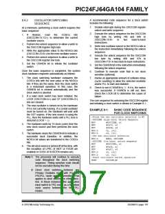
EXAMPLE 8-1:
BASIC CODE SEQUENCE
FOR CLOCK SWITCHING
;Place the new oscillator selection in W0
;OSCCONH (high byte) Unlock Sequence
MOV
MOV
MOV
MOV.b
MOV.b
#OSCCONH, w1
#0x78, w2
#0x9A, w3
w2, [w1]
4. The hardware waits for 10 clock cycles from the
new clock source and then performs the clock
switch.
w3, [w1]
5. The hardware clears the OSWEN bit to indicate a
successful clock transition. In addition, the
NOSCx bit values are transferred to the COSCx
bits.
;Set new oscillator selection
MOV.b WREG, OSCCONH
;OSCCONL (low byte) unlock sequence
MOV
MOV
MOV
MOV.b
MOV.b
#OSCCONL, w1
#0x46, w2
#0x57, w3
w2, [w1]
6. The old clock source is turned off at this time, with
the exception of LPRC (if WDT or FSCM are
enabled) or SOSC (if SOSCEN remains set).
w3, [w1]
Note 1: The processor will continue to execute
code throughout the clock switching
sequence. Timing sensitive code should
not be executed during this time.
;Start oscillator switch operation
BSET OSCCON,#0
2: Direct clock switches between any
Primary Oscillator mode with PLL and
FRCPLL mode are not permitted. This
applies to clock switches in either direc-
tion. In these instances, the application
must switch to FRC mode as a transition
clock source between the two PLL
modes.
2010 Microchip Technology Inc.
DS39951C-page 107

 MICROCHIP [ MICROCHIP ]