PIC24FJ64GA104 FAMILY
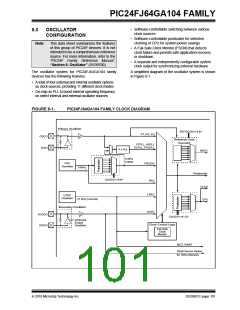
8.1
CPU Clocking Scheme
8.2
Initial Configuration on POR
The system clock source can be provided by one of
four sources:
The oscillator source (and operating mode) that is
used at a device Power-on Reset event is selected
using Configuration bit settings. The oscillator Config-
uration bit settings are located in the Configuration
registers in the program memory (refer to
Section 25.1 “Configuration Bits” for further details).
• Primary Oscillator (POSC) on the OSCI and
OSCO pins
• Secondary Oscillator (SOSC) on the SOSCI and
SOSCO pins
The
Primary
Oscillator
Configuration
bits,
• Fast Internal RC (FRC) Oscillator
POSCMD<1:0> (Configuration Word 2<1:0>), and
the Initial Oscillator Select Configuration bits,
FNOSC<2:0> (Configuration Word 2<10:8>), select
the oscillator source that is used at a Power-on Reset.
The FRC Primary Oscillator with postscaler (FRCDIV)
is the default (unprogrammed) selection. The Second-
ary Oscillator, or one of the internal oscillators, may be
chosen by programming these bit locations.
• Low-Power Internal RC (LPRC) Oscillator
The Primary Oscillator and FRC sources have the
option of using the internal 4x PLL. The frequency of
the FRC clock source can optionally be reduced by the
programmable clock divider. The selected clock source
generates the processor and peripheral clock sources.
The processor clock source is divided by two to pro-
duce the internal instruction cycle clock, FCY. In this
document, the instruction cycle clock is also denoted
by FOSC/2. The internal instruction cycle clock, FOSC/2,
can be provided on the OSCO I/O pin for some
operating modes of the Primary Oscillator.
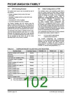
The Configuration bits allow users to choose between
the various clock modes, shown in Table 8-1.
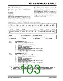
8.2.1
CLOCK SWITCHING MODE
CONFIGURATION BITS
The FCKSM Configuration bits (Configuration
Word 2<7:6>) are used to jointly configure device clock
switching and the Fail-Safe Clock Monitor (FSCM).
Clock switching is enabled only when FCKSM1 is
programmed (‘0’). The FSCM is enabled only when the
FCKSM<1:0> bits are both programmed (‘00’).
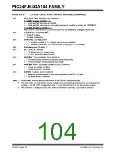
TABLE 8-1:
CONFIGURATION BIT VALUES FOR CLOCK SELECTION
Oscillator Mode
Oscillator Source
POSCMD<1:0>
FNOSC<2:0>
Note
1, 2
Fast RC Oscillator with Postscaler
(FRCDIV)
Internal
11
111
(Reserved)
Internal
Internal
xx
11
11
110
101
100
1
1
1
Low-Power RC Oscillator (LPRC)
Secondary (Timer1) Oscillator
(SOSC)
Secondary
Primary Oscillator (XT) with PLL
Module (XTPLL)
Primary
Primary
01
00
011
011
Primary Oscillator (EC) with PLL
Module (ECPLL)
Primary Oscillator (HS)
Primary Oscillator (XT)
Primary Oscillator (EC)
Primary
Primary
Primary
Internal
10
01
00
11
010
010
010
001
Fast RC Oscillator with PLL Module
(FRCPLL)
1
1
Fast RC Oscillator (FRC)
Internal
11
000
Note 1: OSCO pin function is determined by the OSCIOFCN Configuration bit.
2: This is the default oscillator mode for an unprogrammed (erased) device.
DS39951C-page 102
2010 Microchip Technology Inc.

 MICROCHIP [ MICROCHIP ]