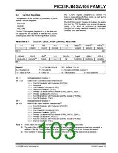
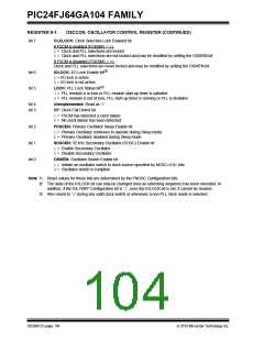
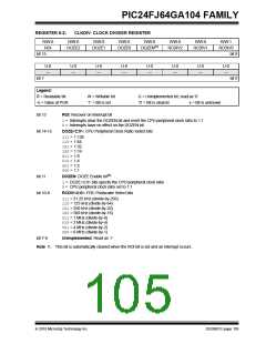
PIC24FJ64GA104 FAMILY
• Software-controllable switching between various
clock sources
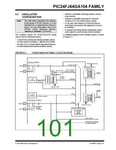
8.0
OSCILLATOR
CONFIGURATION
• Software-controllable postscaler for selective
clocking of CPU for system power savings
Note:
This data sheet summarizes the features
of this group of PIC24F devices. It is not
intended to be a comprehensive reference
source. For more information, refer to the
“PIC24F Family Reference Manual”,
“Section 6. Oscillator” (DS39700).
• A Fail-Safe Clock Monitor (FSCM) that detects
clock failure and permits safe application recovery
or shutdown
• A separate and independently configurable system
clock output for synchronizing external hardware
The oscillator system for PIC24FJ64GA104 family
devices has the following features:
A simplified diagram of the oscillator system is shown
in Figure 8-1.
• A total of four external and internal oscillator options
as clock sources, providing 11 different clock modes
• On-chip 4x PLL to boost internal operating frequency
on select internal and external oscillator sources
FIGURE 8-1:
PIC24FJ64GA104 FAMILY CLOCK DIAGRAM
Primary Oscillator
REFOCON<15:8>
XT, HS, EC
OSCO
OSCI
Reference Clock
Generator
XTPLL, HSPLL
ECPLL,FRCPLL
4 x PLL
REFO
8 MHz
4 MHz
FRC
Oscillator
FRCDIV
8 MHz
(nominal)
Peripherals
CLKDIV<10:8>
FRC
CLKO
CPU
LPRC
LPRC
Oscillator
31 kHz (nominal)
Secondary Oscillator
SOSC
SOSCO
SOSCI
CLKDIV<14:12>
SOSCEN
Enable
Oscillator
Clock Control Logic
Fail-Safe
Clock
Monitor
WDT, PWRT
Clock Source Option
for Other Modules
2010 Microchip Technology Inc.
DS39951C-page 101

 MICROCHIP [ MICROCHIP ]