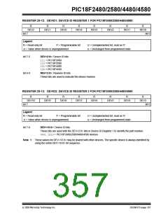
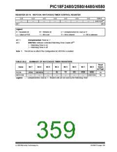
PIC18F2480/2580/4480/4580
To use a higher clock speed on wake-up, the INTOSC
or postscaler clock sources can be selected to provide
25.4 Fail-Safe Clock Monitor
The Fail-Safe Clock Monitor (FSCM) allows the
microcontroller to continue operation in the event of an
external oscillator failure by automatically switching the
device clock to the internal oscillator block. The FSCM
function is enabled by setting the FCMEN Configuration
bit.
a higher clock speed by setting bits, IRCF<2:0>,
immediately after Reset. For wake-ups from Sleep, the
INTOSC or postscaler clock sources can be selected
by setting the IRCF<2:0> bits prior to entering Sleep
mode.
The FSCM will detect failures of the primary or second-
ary clock sources only. If the internal oscillator block
fails, no failure would be detected, nor would any action
be possible.
When FSCM is enabled, the INTRC oscillator runs at
all times to monitor clocks to peripherals and provide a
backup clock in the event of a clock failure. Clock
monitoring (shown in Figure 25-3) is accomplished by
creating a sample clock signal, which is the INTRC out-
put divided by 64. This allows ample time between
FSCM sample clocks for a peripheral clock edge to
occur. The peripheral device clock and the sample
clock are presented as inputs to the Clock Monitor
(CM) latch. The CM is set on the falling edge of the
device clock source, but cleared on the rising edge of
the sample clock.
25.4.1
FSCM AND THE WATCHDOG TIMER
Both the FSCM and the WDT are clocked by the
INTRC oscillator. Since the WDT operates with a
separate divider and counter, disabling the WDT has
no effect on the operation of the INTRC oscillator when
the FSCM is enabled.
As already noted, the clock source is switched to the
INTOSC clock when a clock failure is detected.
Depending on the frequency selected by the
IRCF<2:0> bits, this may mean a substantial change in
the speed of code execution. If the WDT is enabled
with a small prescale value, a decrease in clock speed
allows a WDT time-out to occur and a subsequent
device Reset. For this reason, Fail-Safe Clock events
also reset the WDT and postscaler, allowing it to start
timing from when execution speed was changed and
decreasing the likelihood of an erroneous time-out.
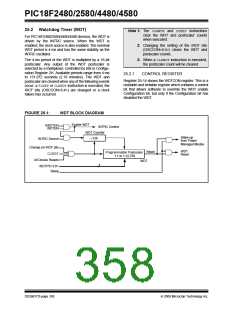
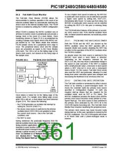
FIGURE 25-3:
FSCM BLOCK DIAGRAM
Clock Monitor
Latch (CM)
(edge-triggered)
Peripheral
Clock
S
C
Q
Q
INTRC
Source
÷ 64
25.4.2
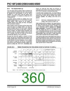
EXITING FAIL-SAFE OPERATION
488 Hz
(2.048 ms)
(32 μs)
The Fail-Safe condition is terminated by either a device
Reset or by entering a power-managed mode. On
Reset, the controller starts the primary clock source
specified in Configuration Register 1H (with any
required start-up delays that are required for the
oscillator mode, such as OST or PLL timer). The
INTOSC multiplexer provides the device clock until the
primary clock source becomes ready (similar to a Two-
Speed Start-up). The clock source is then switched to
the primary clock (indicated by the OSTS bit in the
OSCCON register becoming set). The Fail-Safe Clock
Monitor then resumes monitoring the peripheral clock.
Clock
Failure
Detected
Clock failure is tested for on the falling edge of the
sample clock. If a sample clock falling edge occurs
while CM is still set, a clock failure has been detected
(Figure 25-4). This causes the following:
• the FSCM generates an oscillator fail interrupt by
setting bit, OSCFIF (PIR2<7>);
• the device clock source is switched to the internal
oscillator block (OSCCON is not updated to show
the current clock source – this is the Fail-Safe
condition); and
The primary clock source may never become ready
during start-up. In this case, operation is clocked by the
INTOSC multiplexer. The OSCCON register will remain
in its Reset state until a power-managed mode is
entered.
• the WDT is reset.
During switchover, the postscaler frequency from the
internal oscillator block may not be sufficiently stable for
timing-sensitive applications. In these cases, it may be
desirable to select another clock configuration and enter
an alternate power-managed mode. This can be done to
attempt a partial recovery or execute a controlled shut-
down. See Section 4.1.4 “Multiple Sleep Commands”
and Section 25.3.1 “Special Considerations for
Using Two-Speed Start-up” for more details.
© 2009 Microchip Technology Inc.
DS39637D-page 361

 MICROCHIP [ MICROCHIP ]