PIC18F2480/2580/4480/4580
Each of the five blocks has three code protection bits
associated with them. They are:
25.5 Program Verification and
Code Protection
• Code-Protect bit (CPn)
The overall structure of the code protection on the
PIC18 Flash devices differs significantly from other
PIC® devices.
• Write-Protect bit (WRTn)
• External Block Table Read bit (EBTRn)
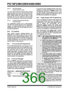
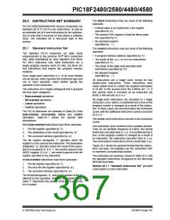
Figure 25-5 shows the program memory organization
for 16 and 32-Kbyte devices and the specific code
protection bit associated with each block. The actual
locations of the bits are summarized in Table 25-3.
The user program memory is divided into five blocks.
One of these is a boot block of 2 Kbytes. The remainder
of the memory is divided into four blocks on binary
boundaries.
FIGURE 25-5:
CODE-PROTECTED PROGRAM MEMORY FOR PIC18F2480/2580/4480/4580
Address
Range
MEMORY SIZE/DEVICE
32 Kbytes
16 Kbytes
Block Code Protection
Controlled by:
(PIC18F2580/4580)
(PIC18F2480/4480)
BBSIZ
0
1
0
1
000000h
0007FFh
000800h
000FFFh
001000h
001FFFh
002000h
Boot Block
1 kW
Boot Block
1 kW
Boot Block
2 kW
Boot Block
2 kW
CPB, WRTB, EBRTB
(Boot Block)
Block 0
3 kW
Block 0
3 kW
Block 0
2 kW
Block 0
2 kW
CP0, WRT0, EBRT0
(Block 0)
Block 1
4 kW
Block 1
4 kW
Block 1
4 kW
Block 1
4 kW
CP!, WRT1, EBRT1
(Block 1)
003FFFh
004000h
Block 2
4 kW
Block 2
4 kW
CP2, WRT2, EBRT2
(Block 2)
005FFFh
006000h
Block 3
4 kW
Block 3
4 kW
CP3, WRT3, EBTR3
(Block 3)
007FFFh
008000h
Unimplemented Unimplemented
Read ‘0’s Read ‘0’s
Unimplemented Unimplemented
Read ‘0’s Read ‘0’s
(Unimplemented Memory Space)
1FFFFFh
© 2009 Microchip Technology Inc.
DS39637D-page 363

 MICROCHIP [ MICROCHIP ]