PIC18F2480/2580/4480/4580
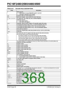
TABLE 25-3: SUMMARY OF CODE PROTECTION REGISTERS
File Name
Bit 7
Bit 6
Bit 5
Bit 4
Bit 3
Bit 2
Bit 1
Bit 0
300008h
CONFIG5L
CONFIG5H
CONFIG6L
—
CPD
—
—
CPB
—
—
—
—
—
—
—
—
—
CP3*
—
CP2
—
CP1
—
CP0
—
300009h
30000Ah
30000Bh
30000Ch
30000Dh
—
WRT3*
—
WRT2
—
WRT1
—
WRT0
—
CONFIG6H WRTD
WRTB
—
WRTC
—
CONFIG7L
CONFIG7H
—
—
EBTR3*
—
EBTR2
—
EBTR1
—
EBTR0
—
EBTRB
—
Legend: Shaded cells are unimplemented.
Unimplemented in PIC18FX480 devices; maintain this bit set.
*
A table read instruction that executes from a location
outside of that block is not allowed to read and will
result in reading ‘0’s. Figures 25-6 through 25-8
illustrate table write and table read protection.
25.5.1
PROGRAM MEMORY
CODE PROTECTION
The program memory may be read to or written from
any location using the table read and table write
instructions. The Device ID may be read with table
reads. The Configuration registers may be read and
written with the table read and table write instructions.
Note:
Code protection bits may only be written to
a ‘0’ from a ‘1’ state. It is not possible to
write a ‘1’ to a bit in the ‘0’ state. Code
protection bits are only set to ‘1’ by a full
chip erase or block erase function. The full
chip erase and block erase functions can
only be initiated via ICSP or an external
programmer.
In normal execution mode, the CPn bits have no direct
effect. CPn bits inhibit external reads and writes. A
block of user memory may be protected from table
writes if the WRTn Configuration bit is ‘0’. The EBTRn
bits control table reads. For a block of user memory
with the EBTRn bit set to ‘0’, a table read instruction
that executes from within that block is allowed to read.
FIGURE 25-6:
TABLE WRITE (WRTn) DISALLOWED
Register Values
Program Memory
Configuration Bit Settings
000000h
WRTB, EBTRB = 11
0007FFh
000800h
TBLPTR = 0008FFh
PC = 003FFEh
WRT0, EBTR0 = 01
TBLWT*
TBLWT*
003FFFh
004000h
WRT1, EBTR1 = 11
WRT2, EBTR2 = 11
WRT3, EBTR3 = 11
007FFFh
008000h
PC = 00BFFEh
00BFFFh
00C000h
00FFFFh
Results: All table writes disabled to Blockn whenever WRTn = 0.
DS39637D-page 364
© 2009 Microchip Technology Inc.

 MICROCHIP [ MICROCHIP ]