PIC18F2480/2580/4480/4580
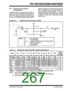
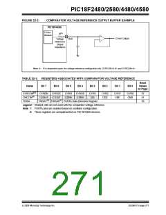
FIGURE 22-2:
COMPARATOR VOLTAGE REFERENCE OUTPUT BUFFER EXAMPLE
PIC18F4X80
CVREF
Module
(1)
R
+
–
CVREF Output
RA0
Voltage
Reference
Output
Impedance
Note 1: R is dependent upon the voltage reference configuration bits, CVRCON<3:0> and CVRCON<5>.
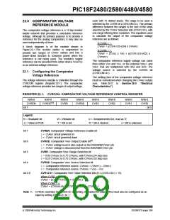
TABLE 22-1: REGISTERS ASSOCIATED WITH COMPARATOR VOLTAGE REFERENCE
Reset
Values
Name
Bit 7
Bit 6
Bit 5
Bit 4
Bit 3
Bit 2
Bit 1
Bit 0
on Page:
CVRCON(2)
CMCON(2)
TRISA
CVREN
C2OUT
CVROE
C1OUT
CVRR
C2INV
CVRSS
C1INV
CVR3
CIS
CVR2
CM2
CVR1
CM1
CVR0
CM0
57
57
58
TRISA7(1) TRISA6(1) PORTA Data Direction Register
Legend: Shaded cells are not used with the comparator voltage reference.
Note 1: PORTA pins are enabled based on oscillator configuration.
2: These registers are unimplemented on PIC18F2X80 devices.
© 2009 Microchip Technology Inc.
DS39637D-page 271

 MICROCHIP [ MICROCHIP ]