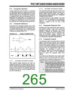
PIC18F2480/2580/4480/4580
each with 16 distinct levels. The range to be used is
selected by the CVRR bit (CVRCON<5>). The primary
difference between the ranges is the size of the steps
22.0 COMPARATOR VOLTAGE
REFERENCE MODULE
selected by the CVREF Selection bits (CVR<3:0>), with
one range offering finer resolution. The equations used
to calculate the output of the comparator voltage
reference are as follows:
The comparator voltage reference is a 16-tap resistor
ladder network that provides a selectable reference
voltage. Although its primary purpose is to provide a
reference for the analog comparators, it may also be
used independently of them.
If CVRR = 1:
CVREF = ((CVR<3:0>)/24) x CVRSRC
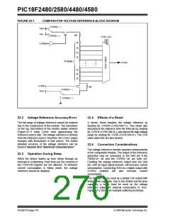
A
block diagram is of the module shown in
Figure 22-1.The resistor ladder is segmented to
provide two ranges of CVREF values and has a
power-down function to conserve power when the
reference is not being used. The module’s supply
reference can be provided from either device VDD/VSS
or an external voltage reference.
If CVRR = 0:
CVREF = (CVDD x 1/4) + (((CVR<3:0>)/32) x
CVRSRC)
The comparator reference supply voltage can come
from either VDD and VSS, or the external VREF+ and
VREF- that are multiplexed with RA2 and RA3. The
voltage source is selected by the CVRSS bit
(CVRCON<4>).
22.1 Configuring the Comparator
Voltage Reference
The settling time of the comparator voltage reference
must be considered when changing the CVREF output
(see Table 28-3 in Section 28.0 “Electrical
Characteristics”).
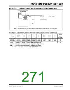
The voltage reference module is controlled through the
CVRCON register (Register 22-1). The comparator
voltage reference provides two ranges of output voltage,
REGISTER 22-1: CVRCON: COMPARATOR VOLTAGE REFERENCE CONTROL REGISTER
R/W-0
R/W-0
CVROE(1)
R/W-0
CVRR
R/W-0
R/W-0
CVR3
R/W-0
CVR2
R/W-0
CVR1
R/W-0
CVR0
CVREN
CVRSS
bit 7
bit 0
Legend:
R = Readable bit
W = Writable bit
‘1’ = Bit is set
U = Unimplemented bit, read as ‘0’
‘0’ = Bit is cleared x = Bit is unknown
-n = Value at POR
bit 7
bit 6
bit 5
bit 4
bit 3-0
CVREN: Comparator Voltage Reference Enable bit
1= CVREF circuit powered on
0= CVREF circuit powered down
CVROE: Comparator VREF Output Enable bit(1)
1= CVREF voltage level is also output on the RA0/AN0/CVREF pin
0= CVREF voltage is disconnected from the RA0/AN0/CVREF pin
CVRR: Comparator VREF Range Selection bit
1= 0.00 CVRSRC to 0.75 CVRSRC, with CVRSRC/24 step size
0= 0.25 CVRSRC to 0.75 CVRSRC, with CVRSRC/32 step size
CVRSS: Comparator VREF Source Selection bit
1= Comparator reference source, CVRSRC = (VREF+) – (VREF-)
0= Comparator reference source, CVRSRC = VDD – VSS
CVR<3:0>: Comparator VREF Value Selection bits (0 ≤ (CVR<3:0>) ≤ 15)
When CVRR = 1:
CVREF = ((CVR<3:0>)/24) • (CVRSRC)
When CVRR = 0:
CVREF = (CVRSRC/4) + ((CVR<3:0>)/32) • (CVRSRC)
Note 1: CVROE overrides the TRISA<0> bit setting. If enabled for output, RA2 must also be configured as an
input by setting TRISA<2> to ‘1’.
© 2009 Microchip Technology Inc.
DS39637D-page 269

 MICROCHIP [ MICROCHIP ]