PIC18F2480/2580/4480/4580
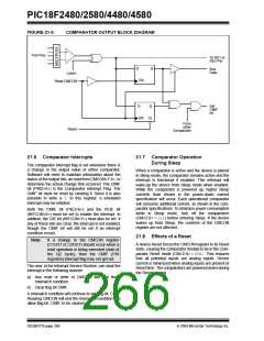
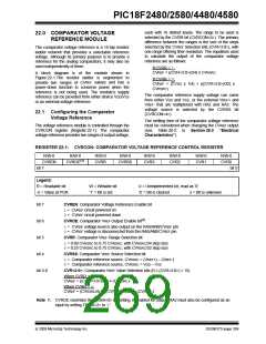
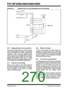
FIGURE 22-1:
COMPARATOR VOLTAGE REFERENCE BLOCK DIAGRAM
CVRSS = 1
CVRSS = 0
VREF+
VDD
8R
CVR<3:0>
R
CVREN
R
R
R
16 Steps
CVREF
R
R
R
CVRR
VREF-
8R
CVRSS = 1
CVRSS = 0
22.2 Voltage Reference Accuracy/Error
22.4 Effects of a Reset
The full range of voltage reference cannot be realized
due to the construction of the module. The transistors
on the top and bottom of the resistor ladder network
(Figure 22-1) keep CVREF from approaching the
reference source rails. The voltage reference is derived
from the reference source; therefore, the CVREF output
changes with fluctuations in that source. The tested
absolute accuracy of the voltage reference can be
found in Section 28.0 “Electrical Characteristics”.
A device Reset disables the voltage reference by
clearing bit, CVREN (CVRCON<7>). This Reset also
disconnects the reference from the RA0 pin by clearing
bit, CVROE (CVRCON<6>), and selects the high-voltage
range by clearing bit, CVRR (CVRCON<5>). The CVR
value select bits are also cleared.
22.5 Connection Considerations
The voltage reference module operates independently
of the comparator module. The output of the reference
generator may be connected to the RA0 pin if the
TRISA<0> bit and the CVROE bit are both set.
Enabling the voltage reference output onto the RA0
pin, with an input signal present, will increase current
consumption. Connecting RA0 as a digital output with
CVRSS enabled will also increase current
consumption.
22.3 Operation During Sleep
When the device wakes up from Sleep through an
interrupt or a Watchdog Timer time-out, the contents of
the CVRCON register are not affected. To minimize
current consumption in Sleep mode, the voltage
reference should be disabled.
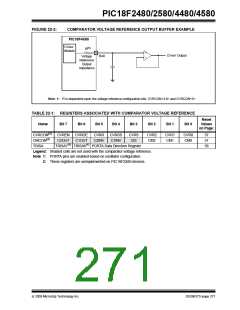
The RA0 pin can be used as a simple D/A output with
limited drive capability. Due to the limited current drive
capability, a buffer must be used on the voltage
reference output for external connections to VREF.
Figure 22-2 shows an example buffering technique.
DS39637D-page 270
© 2009 Microchip Technology Inc.

 MICROCHIP [ MICROCHIP ]