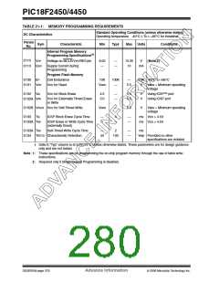
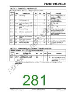
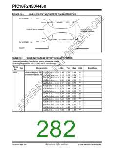
PIC18F2450/4450
21.4.2
TIMING CONDITIONS
Note:
Because of space limitations, the generic
terms “PIC18FXXXX” and “PIC18LFXXXX”
are used throughout this section to refer to
the PIC18F2450/4450 and PIC18LF2450/
4450 families of devices specifically and
only those devices.
The temperature and voltages specified in Table 21-5
apply to all timing specifications unless otherwise
noted. Figure 21-4 specifies the load conditions for the
timing specifications.
TABLE 21-5: TEMPERATURE AND VOLTAGE SPECIFICATIONS – AC
Standard Operating Conditions (unless otherwise stated)
Operating temperature
-40°C ≤ TA ≤ +85°C for industrial
AC CHARACTERISTICS
Operating voltage VDD range as described in DC spec Section 21.1 and
Section 21.3 .
LF parts operate for industrial temperatures only.
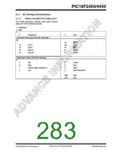
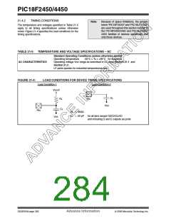
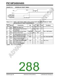
FIGURE 21-4:
LOAD CONDITIONS FOR DEVICE TIMING SPECIFICATIONS
Load Condition 1 Load Condition 2
VDD/2
CL
RL
Pin
VSS
CL
Pin
RL = 464Ω
CL = 50 pF for all pins except OSC2/CLKO
and including D and E outputs as ports
VSS
DS39760A-page 282
Advance Information
© 2006 Microchip Technology Inc.

 MICROCHIP [ MICROCHIP ]