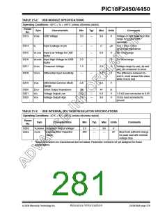
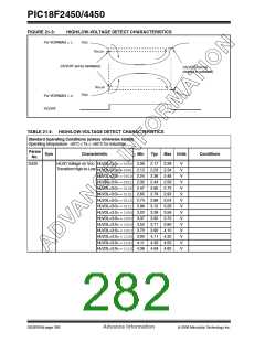
PIC18F2450/4450
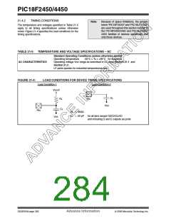
21.4.3
TIMING DIAGRAMS AND SPECIFICATIONS
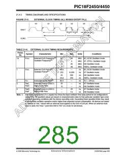
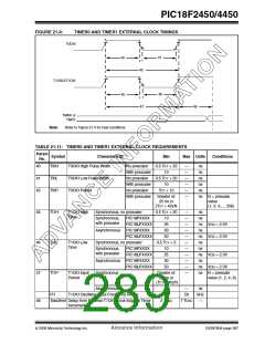
FIGURE 21-5:
EXTERNAL CLOCK TIMING (ALL MODES EXCEPT PLL)
Q4
Q1
1
Q2
Q3
Q4
Q1
OSC1
CLKO
3
4
3
4
2
TABLE 21-6: EXTERNAL CLOCK TIMING REQUIREMENTS
Param.
Symbol
Characteristic
Min
Max
Units
Conditions
No.
1A
FOSC
External CLKI Frequency(1)
Oscillator Frequency(1)
DC
0.1
4
48
4
MHz EC, ECIO Oscillator mode
MHz XT, XTPLL Oscillator mode
MHz HS Oscillator mode
25
4
48
MHz HSPLL Oscillator mode
1
TOSC
TCY
External CLKI Period(1)
Oscillator Period(1)
20.8
250
25
—
ns
ns
ns
ns
ns
ns
ns
ns
ns
EC, ECIO Oscillator mode
XT Oscillator mode
HS Oscillator mode
HSPLL Oscillator mode
TCY = 4/FOSC
10,000
250
250
—
20.8
83.3
30
2
3
Instruction Cycle Time(1)
TosL,
TosH
External Clock in (OSC1)
High or Low Time
—
XT Oscillator mode
HS Oscillator mode
XT Oscillator mode
HS Oscillator mode
10
—
4
TosR,
TosF
External Clock in (OSC1)
Rise or Fall Time
—
20
—
7.5
Note 1: Instruction cycle period (TCY) equals four times the input oscillator time base period for all configurations
except PLL. All specified values are based on characterization data for that particular oscillator type under
standard operating conditions with the device executing code. Exceeding these specified limits may result
in an unstable oscillator operation and/or higher than expected current consumption. All devices are tested
to operate at “min.” values with an external clock applied to the OSC1/CLKI pin. When an external clock
input is used, the “max.” cycle time limit is “DC” (no clock) for all devices.
© 2006 Microchip Technology Inc.
Advance Information
DS39760A-page 283

 MICROCHIP [ MICROCHIP ]