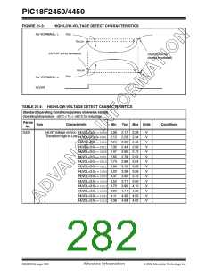
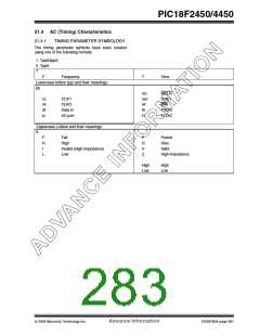
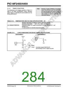
PIC18F2450/4450
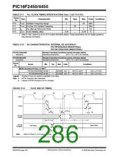
TABLE 21-7: PLL CLOCK TIMING SPECIFICATIONS (VDD = 4.2V TO 5.5V)
Param
Sym
Characteristic
Min
Typ†
Max
Units Conditions
No.
F10
FOSC Oscillator Frequency Range
4
—
—
96
—
—
48
—
MHz
MHz
ms
F11
F12
F13
FSYS On-Chip VCO System Frequency
trc
PLL Start-up Time (Lock Time)
—
2
ΔCLK CLKO Stability (Jitter)
-0.25
+0.25
%
†
Data in “Typ” column is at 5V, 25°C unless otherwise stated. These parameters are for design guidance
only and are not tested.
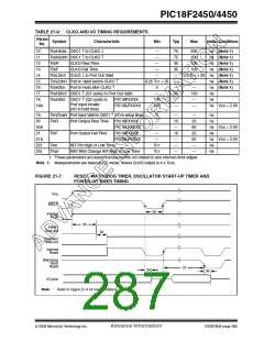
TABLE 21-8: AC CHARACTERISTICS: INTERNAL RC ACCURACY
PIC18F2450/4450 (INDUSTRIAL)
PIC18LF2450/4450 (INDUSTRIAL)
PIC18LF2450/4450
Standard Operating Conditions (unless otherwise stated)
Operating temperature -40°C ≤ TA ≤ +85°C for industrial
(Industrial)
PIC18F2450/4450
Standard Operating Conditions (unless otherwise stated)
Operating temperature -40°C ≤ TA ≤ +85°C for industrial
(Industrial)
Param
No.
Device
Min
Typ
Max
Units
Conditions
(1)
INTRC Accuracy @ Freq = 31 kHz
PIC18LF2450/4450 26.562
PIC18F2450/4450 26.562
—
—
35.938
35.938
kHz
kHz
-40°C to +85°C
-40°C to +85°C
VDD = 2.7-3.3V
VDD = 4.5-5.5V
Legend:
Shading of rows is to assist in readability of the table.
Note 1: INTRC frequency after calibration.
2: Change of INTRC frequency as VDD changes.
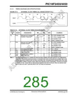
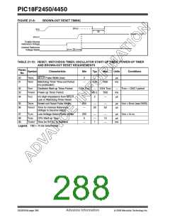
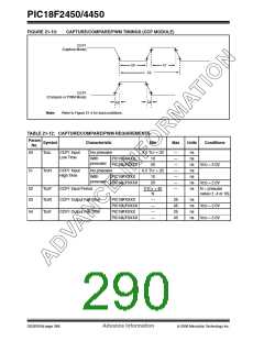
FIGURE 21-6:
CLKO AND I/O TIMING
Q1
Q2
Q3
Q4
OSC1
11
10
CLKO
12
13
14
18
19
16
I/O pin
(Input)
15
17
I/O pin
(Output)
New Value
Old Value
20, 21
Refer to Figure 21-4 for load conditions.
Note:
DS39760A-page 284
Advance Information
© 2006 Microchip Technology Inc.

 MICROCHIP [ MICROCHIP ]