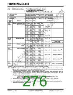
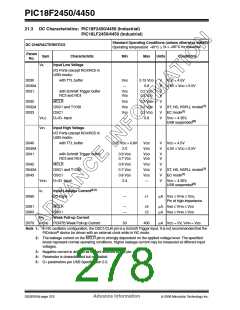
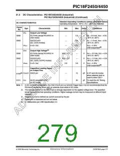
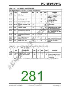
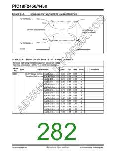
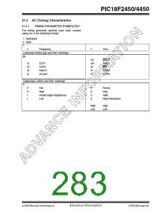
PIC18F2450/4450
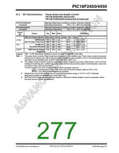
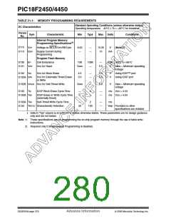
TABLE 21-1: MEMORY PROGRAMMING REQUIREMENTS
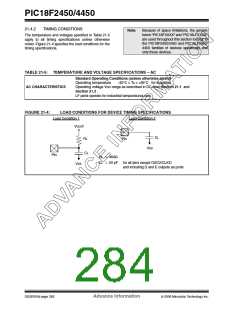
Standard Operating Conditions (unless otherwise stated)
Operating temperature -40°C ≤ TA ≤ +85°C for industrial
DC Characteristics
Param
Sym
No.
Characteristic
Min
Typ†
Max
Units
Conditions
Internal Program Memory
Programming Specifications(1)
D110
D113
VPP
Voltage on MCLR/VPP/RE3 pin
9.00
—
—
—
13.25
10
V
(Note 2)
IDDP
Supply Current during
Programming
mA
Program Flash Memory
Cell Endurance
D130
D131
EP
10K
100K
—
—
E/W -40°C to +85°C
VPR
VDD for Read
VMIN
5.5
V
VMIN = Minimum operating
voltage
D132
VIE
VDD for Block Erase
4.5
3.0
—
—
5.5
5.5
V
V
Using ICSP™ port
Using ICSP port
D132A VIW
VDD for Externally Timed Erase
or Write
D132B VPEW VDD for Self-Timed Write
VMIN
—
5.5
V
VMIN = Minimum operating
voltage
D133
TIE
ICSP Block Erase Cycle Time
—
1
4
—
—
ms VDD > 4.5V
ms VDD > 4.5V
D133A TIW
ICSP Erase or Write Cycle Time
(externally timed)
—
D133A TIW
Self-Timed Write Cycle Time
—
2
—
—
ms
D134 TRETD Characteristic Retention
40
100
Year Provided no other
specifications are violated
†
Data in “Typ” column is at 5.0V, 25°C unless otherwise stated. These parameters are for design guidance
only and are not tested.
Note 1: These specifications are for programming the on-chip program memory through the use of table write
instructions.
2: Required only if Single-Supply Programming is disabled.
DS39760A-page 278
Advance Information
© 2006 Microchip Technology Inc.

 MICROCHIP [ MICROCHIP ]