PIC18F2450/4450
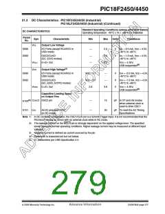
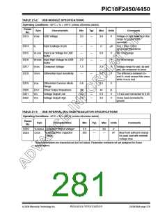
TABLE 21-2: USB MODULE SPECIFICATIONS
Operating Conditions: -40°C < TA < +85°C (unless otherwise stated).
Param
Sym
Characteristic
USB Voltage
Min
Typ
Max
Units
Comments
No.
D313
VUSB
3.0
—
3.6
V
Voltage on bus must be in this
range for proper USB
operation
D314
D315
D316
D317
D318
IIL
Input Leakage on pin
—
—
—
—
—
1
0.8
—
μA
V
VSS ≤ VPAD ≤ VDD;
pin at high impedance
VILUSB Input Low Voltage for USB
Buffer
For VUSB range
For VUSB range
VIHUSB Input High Voltage for USB
Buffer
2.0
1.3
—
V
VCRS
Crossover Voltage
2.0
0.2
V
Voltage range for pad_dp and
pad_dm crossover to occur
VDIFS
Differential Input Sensitivity
—
—
V
The difference between D+
and D- must exceed this value
while VCM is met
D319
VCM
Differential Common Mode
Range
0.8
2.5
V
D320
D321
D322
ZOUT
VOL
Driver Output Impedance
Voltage Output Low
28
0.0
2.8
—
—
—
44
0.3
3.6
Ω
V
V
1.5 kΩ load connected to 3.6V
VOH
Voltage Output High
15 kΩ load connected to
ground
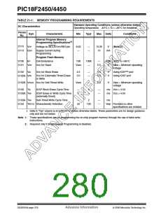
TABLE 21-3: USB INTERNAL VOLTAGE REGULATOR SPECIFICATIONS
Operating Conditions: -40°C < TA < +85°C (unless otherwise stated).
Param
Sym
Characteristics
Min
Typ
Max
Units
Comments
No.
D323
D324
VUSBANA Regulator Output Voltage*
3.0
—
—
3.6
—
V
CUSB
External Filter Capacitor
Value*
220
nF
Must hold sufficient charge
for peak load with minimal
voltage drop
*
These parameters are characterized but not tested. Parameter numbers not yet assigned for these
specifications.
© 2006 Microchip Technology Inc.
Advance Information
DS39760A-page 279

 MICROCHIP [ MICROCHIP ]