PIC18CXX2
8.5
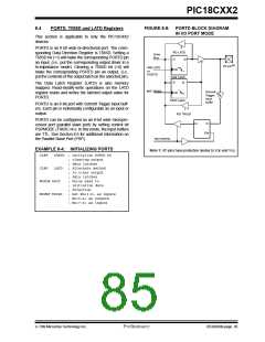
PORTE, TRISE and LATE Registers
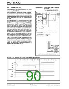
FIGURE 8-9: PORTE BLOCK DIAGRAM
IN I/O PORT MODE
This section is only applicable to the PIC18C4X2
devices.
PORTE is an 3 bit wide bi-directional port. The corre-
sponding Data Direction Register is TRISE. Setting a
TRISE bit (=1) will make the corresponding PORTE pin
an input, (i.e., put the corresponding output driver in a
hi-impedance mode). Clearing a TRISE bit (=0) will
make the corresponding PORTE pin an output, (i.e.,
put the contents of the output latch on the selected pin).
RD LATE
Data
Bus
D
Q
I/O pin(1)
WR LATE
or
PORTE
CK
Data Latch
The Data Latch Register (LATE) is also memory
mapped. Read-modify-write operations on the LATE
register reads and writes the latched output value for
PORTE.
D
Q
WR TRISE
Schmitt
Trigger
input
CK
TRIS Latch
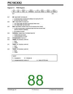
PORTE has three pins RE0/RD/AN5, RE1/WR/AN6
and RE2/CS/AN7, which are individually configurable
as inputs or outputs. These pins have Schmitt Trigger
input buffers.
buffer
RD TRISE
Figure 8-1 shows the TRISE register, which also con-
trols the parallel slave port operation. Capture2 input/
Compare2 output/PWM output when CCP2MX config-
uration bit is enabled.
Q
D
EN
EN
PORTE pins are multiplexed with analog inputs. When
selected as an analog input, these pins will read as ’0’s.
RD PORTE
TRISE controls the direction of the RE pins, even when
they are being used as analog inputs. The user must
make sure to keep the pins configured as inputs when
using them as analog inputs.
To Analog Converter
Note 1: I/O pins have protection diodes to VDD and VSS.
Note: On a Power-on Reset, these pins are con-
figured as analog inputs.
EXAMPLE 8-5: INITIALIZING PORTE
CLRF
PORTE
; Initialize PORTE by
; clearing output
; data latches
CLRF
LATE
; Alternate method
; to clear output
; data latches
MOVLW 0x07
; Configure A/D
MOVWF ADCON1 ; for digital inputs
MOVLW 0x03
; Value used to
; initialize data
; direction
MOVWF TRISC
; Set RE<0> as inputs
; RE<1> as outputs
; RE<2> as inputs
7/99 Microchip Technology Inc.
Preliminary
DS39026B-page 87

 MICROCHIP [ MICROCHIP ]