PIC18CXX2
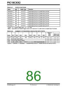
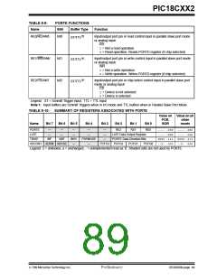
TABLE 8-9:
Name
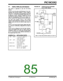
PORTE FUNCTIONS
Bit#
Buffer Type
Function
ST/TTL(1)
RE0/RD/AN5
RE1/WR/AN6
RE2/CS/AN7
bit0
Input/output port pin or read control input in parallel slave port mode
or analog input:
RD
1= Not a read operation
0= Read operation. Reads PORTD register (if chip selected)
ST/TTL(1)
ST/TTL(1)
bit1
bit2
Input/output port pin or write control input in parallel slave port mode
or analog input:
WR
1= Not a write operation
0= Write operation. Writes PORTD register (if chip selected)
Input/output port pin or chip select control input in parallel slave port
mode or analog input:
CS
1= Device is not selected
0= Device is selected
Legend: ST = Schmitt Trigger input, TTL = TTL input
Note 1: Input buffers are Schmitt Triggers when in I/O mode and TTL buffers when in Parallel Slave Port Mode.
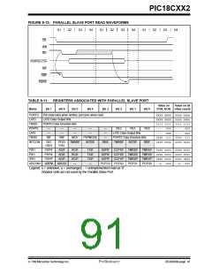
TABLE 8-10: SUMMARY OF REGISTERS ASSOCIATED WITH PORTE
Value on Value on all
POR,
BOR
other
resets
Name
Bit 7
Bit 6
Bit 5
Bit 4
Bit 3
Bit 2
Bit 1
Bit 0
PORTE
LATE
—
—
—
—
—
—
—
—
—
RE2
RE1
RE0
---- -000
---- -xxx
0000 -111
--0- -000
---- -000
---- -uuu
0000 -111
--0- -000
—
PSPMODE
—
LATE Data Output Register
PORTE Data Direction Bits
TRISE
IBF
OBF
IBOV
—
—
ADCON1 ADFM ADCS2
PCFG3
PCFG2
PCFG1
PCFG0
Legend: x = unknown, u = unchanged, - = unimplemented read as ’0’. Shaded cells are not used by PORTE.
7/99 Microchip Technology Inc.
Preliminary
DS39026B-page 89

 MICROCHIP [ MICROCHIP ]