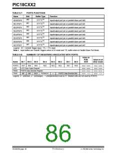
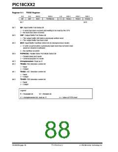
PIC18CXX2
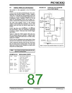
8.6
Parallel Slave Port
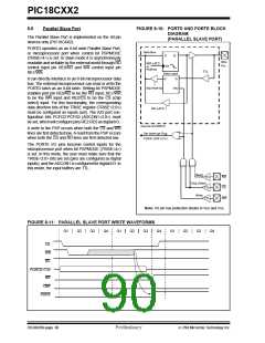
FIGURE 8-10: PORTD AND PORTE BLOCK
DIAGRAM
The Parallel Slave Port is implemented on the 40-pin
devices only (PIC18C4X2).
(PARALLEL SLAVE PORT)
PORTD operates as an 8-bit wide Parallel Slave Port,
or microprocessor port when control bit PSPMODE
(TRISE<4>) is set. In slave mode it is asynchronously
readable and writable by the external world through RD
control input pin RE0/RD and WR control input pin
RE1/WR.
Data Bus
D
Q
RDx
Pin
WR LATD
or
PORTD
CK
Data Latch
TTL
Q
D
It can directly interface to an 8-bit microprocessor data
bus. The external microprocessor can read or write the
PORTD latch as an 8-bit latch. Setting bit PSPMODE
enables port pin RE0/RD to be the RD input, RE1/WR
to be the WR input and RE2/CS to be the CS (chip
select) input. For this functionality, the corresponding
data direction bits of the TRISE register (TRISE<2:0>)
must be configured as inputs (set). The A/D port con-
figuration bits PCFG2:PCFG0 (ADCON1<2:0>) must
be set, which will configure pins RE2:RE0 as digital I/O.
RD PORTD
EN
EN
RD LATD
One bit of PORTD
A write to the PSP occurs when both the CS and WR
lines are first detected low. A read from the PSP occurs
when both the CS and RD lines are first detected low.
Set Interrupt Flag
PSPIF (PIR1<7>)
The PORTE I/O pins become control inputs for the
microprocessor port when bit PSPMODE (TRISE<4>)
is set. In this mode, the user must make sure that the
TRISE<2:0> bits are set (pins are configured as digital
inputs), and the ADCON1 is configured for digital I/O. In
this mode, the input buffers are TTL.
Read
RD
CS
WR
TTL
Chip Select
TTL
Write
TTL
Note: I/O pin has protection diodes to VDD and VSS.
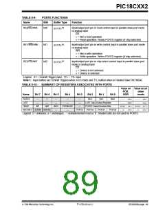
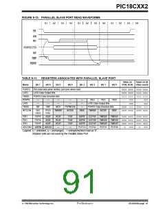
FIGURE 8-11: PARALLEL SLAVE PORT WRITE WAVEFORMS
Q1
Q2
Q3
Q4
Q1
Q2
Q3
Q4
Q1
Q2
Q3
Q4
CS
WR
RD
PORTD<7:0>
IBF
OBF
PSPIF
DS39026B-page 90
Preliminary
7/99 Microchip Technology Inc.

 MICROCHIP [ MICROCHIP ]