PIC18CXX2
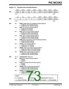
Register 7-6: Peripheral Interrupt Enable Registers
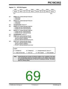
R/W-0
PSPIE
R/W-0
ADIE
R/W-0
RCIE
R/W-0
TXIE
R/W-0
SSPIE
R/W-0
R/W-0
R/W-0
PIE1
CCP1IE TMR2IE TMR1IE
bit 0
bit 7
U-0
U-0
U-0
U-0
R/W-0
R/W-0
R/W-0
R/W-0
PIE2
PIE1
—
—
—
—
BCLIE
LVDIE
TMR3IE CCP2IE
bit 0
bit 7
bit 7
PSPIE: Parallel Slave Port Read/Write Interrupt Enable bit
1= Enables the PSP read/write interrupt
0= Disables the PSP read/write interrupt
bit 6
bit 5
bit 4
bit 3
bit 2
bit 1
bit 0
ADIE: A/D Converter Interrupt Enable bit
1= Enables the A/D interrupt
0= Disables the A/D interrupt
RCIE: USART Receive Interrupt Enable bit
1= Enables the USART receive interrupt
0= Disables the USART receive interrupt
TXIE: USART Transmit Interrupt Enable bit
1= Enables the USART transmit interrupt
0= Disables the USART transmit interrupt
SSPIE: Master Synchronous Serial Port Interrupt Enable bit
1= Enables the MSSP interrupt
0= Disables the MSSP interrupt
CCP1IE: CCP1 Interrupt Enable bit
1= Enables the CCP1 interrupt
0= Disables the CCP1 interrupt
TMR2IE: TMR2 to PR2 Match Interrupt Enable bit
1= Enables the TMR2 to PR2 match interrupt
0= Disables the TMR2 to PR2 match interrupt
TMR1IE: TMR1 Overflow Interrupt Enable bit
1= Enables the TMR1 overflow interrupt
0= Disables the TMR1 overflow interrupt
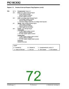
PIE2
bit 7-4
bit 3
Unimplemented: Read as '0'
BCLIE: Bus Collision Interrupt Enable bit
1= Enabled
0= Disabled
bit 2
bit 1
bit 0
LVDIE: Low-voltage Detect Interrupt Enable bit
1= Enabled
0= Disabled
TMR3IE: TMR3 Overflow Interrupt Enable bit
1= Enables the TMR3 overflow interrupt
0= Disables the TMR3 overflow interrupt
CCP2IE: CCP2 Interrupt Enable bit
1= Enables the CCP2 interrupt
0= Disables the CCP2 interrupt
Legend:
R = Readable bit
W = Writable bit
’1’ = Bit is set
U = Unimplemented bit, read as ‘0’
’0’ = Bit is cleared x = Bit is unknown
- n = Value at POR reset
7/99 Microchip Technology Inc.
Preliminary
DS39026B-page 73

 MICROCHIP [ MICROCHIP ]