PIC18CXX2
5.1.1
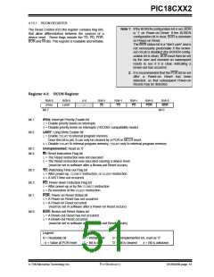
RCON REGISTER
5.1
Control Registers
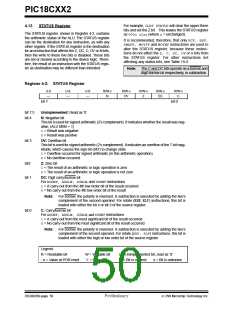
The LWRT bit specifies the operation of Table Writes to
internal memory when the VPP voltage is applied to the
MCLR pin. When the LWRT bit is set, the controller
continues to execute user code, but long table writes
are allowed (for programming internal program mem-
ory) from user mode. The LWRT bit can be cleared only
by performing either a POR or MCLR reset.
Several control registers are used in conjunction with
the TBLRDand TBLWTinstructions. These include the:
• TBLPTR registers
• TABLAT register
• RCON register
Register 5-1: RCON Register (Address: 08h)
R/W-0
IPEN
R/W-0
LWRT
U-0
R/W-1
R/W-1
R/W-1
R/W-0
R/W-0
—
RI
TO
PD
POR
BOR
bit 7
bit 0
bit 7
bit 6
IPEN: Interrupt Priority Enable
1= Enable priority levels on interrupts
0= Disable priority levels on interrupts (16CXXX compatibility mode)
LWRT: Long Write Enable
1= Enable TBLWT to internal program memory
0= Disable TBLWT to internal program memory.
Note 1: Only cleared on a POR or MCLR reset.
This bit has no effect on TBLWTsto external program memory.
bit 5
bit 4
Unimplemented: Read as ’0’
RI: Reset Instruction Flag bit
1= No Reset instruction occurred
0= A Reset instruction occurred
bit 3
bit 2
bit 1
bit 0
TO: Time-out bit
1= After power-up, CLRWDTinstruction, or SLEEPinstruction
0= A WDT time-out occurred
PD: Power-down bit
1= After power-up or by the CLRWDTinstruction
0= By execution of the SLEEPinstruction
POR: Power-on Reset Status bit
1= No Power-on Reset occurred
0= A Power-on Reset occurred (must be set in software after a Power-on Reset occurs)
BOR: Brown-out Reset Status bit
1= No Brown-out Reset nor POR reset occurred
0= A Brown-out Reset nor POR reset occurred
(must be set in software after a Brown-out Reset occurs)
Legend:
R = Readable bit
W = Writable bit
U = Unimplemented bit, read as ‘0’
’0’ = Bit is cleared x = Bit is unknown
- n = Value at POR reset
’1’ = Bit is set
DS39026B-page 54
Preliminary
7/99 Microchip Technology Inc.

 MICROCHIP [ MICROCHIP ]