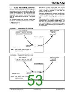
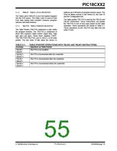
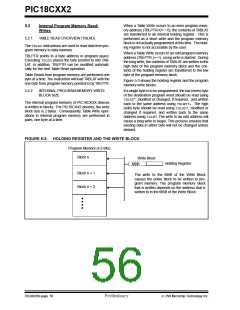
PIC18CXX2
5.2.2.1
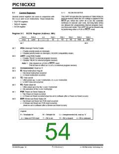
OPERATION
5.2.2.2
SEQUENCE OF EVENTS
The long write is what actually programs words of data
into the internal memory. When a TBLWTto the MSB of
the write block occurs, instruction execution is halted.
During this time, programming voltage and the data
stored in internal latches is applied to program memory.
The sequence of events for programming an internal
program memory location should be:
1. Enable the interrupt that terminates the long
write. Disable all other interrupts.
2. Clear the source interrupt flag.
For a long write to occur:
3. If Interrupt Service Routine execution is desired
when the device wakes, enable global inter-
rupts.
1. MCLR/VPP pin must be at the programming volt-
age
2. LWRT bit must be set
4. Set LWRT bit in the RCON register.
3. TBLWT to the address of the MSB of the write
block
5. Raise MCLR/VPP pin to the programming volt-
age, VPP.
6. Clear the WDT (if enabled).
If the LWRT bit is clear, a short write will occur and pro-
gram memory will not be changed. If the TBLWTis not
to the MSB of the write block, then the programming
phase is not initiated.
7. Set the interrupt source to interrupt at the
required time.
8. Execute the table write for the lower (even) byte.
This will be a short write.
Setting the LWRT bit enables long writes when the
MCLR pin is taken to VPP voltage. Once the LWRT bit
is set, it can be cleared only by performing a POR or
MCLR reset.
9. Execute the table write for the upper (odd) byte.
This will be a long write. The controller will go to
sleep while programming. The interrupt wakes
the controller.
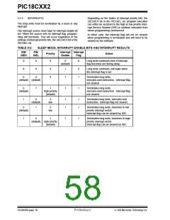
To ensure that the memory location has been well pro-
grammed, a minimum programming time is required.
The long write can be terminated after the program-
ming time has expired by a reset or an interrupt. Having
only one interrupt source enabled to terminate the long
write ensures that no unintended interrupts will prema-
turely terminate the long write.
10. If GIE was set, service the interrupt request.
11. Lower MCLR/VPP pin to VDD.
12. Verify the memory location (table read).
7/99 Microchip Technology Inc.
Preliminary
DS39026B-page 57

 MICROCHIP [ MICROCHIP ]