PIC18CXX2
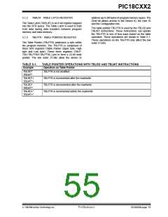
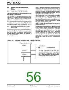
When a Table Write occurs to an even program mem-
ory address (TBLPTR<0> = 0), the contents of TABLAT
are transferred to an internal holding register. This is
performed as a short write and the program memory
block is not actually programmed at this time. The hold-
ing register is not accessible by the user.
5.2
Internal Program Memory Read/
Writes
5.2.1
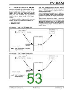
TABLE READ OVERVIEW (TBLRD)
The TBLRDinstructions are used to read data from pro-
gram memory to data memory.
When a Table Write occurs to an odd program memory
address (TBLPTR,)>=1), a long write is started. During
the long write, the contents of TABLAT are written to the
high byte of the program memory block and the con-
tents of the holding register are transferred to the low
byte of the program memory block.
TBLPTR points to a byte address in program space.
Executing TBLRDplaces the byte pointed to into TAB-
LAT. In addition, TBLPTR can be modified automati-
cally for the next Table Read operation.
Table Reads from program memory are performed one
byte at a time. The instruction will load TABLAT with the
one byte from program memory pointed to by TBLPTR.
Figure 5-3 shows the holding register and the program
memory write blocks.
5.2.2
INTERNAL PROGRAM MEMORY WRITE
BLOCK SIZE
If a single byte is to be programmed, the low (even) byte
of the destination program word should be read using
TBLRD*, modified or changed, if required, and written
back to the same address using TBLWT*+. The high
(odd) byte should be read using TBLRD*, modified or
changed if required, and written back to the same
address using TBLWT. The write to an odd address will
cause a long write to begin. This process ensures that
existing data in either byte will not be changed unless
desired.
The internal program memory of PIC18CXXX devices
is written in blocks. For PIC18CXX2 devices, the write
block size is 2 bytes. Consequently, Table Write oper-
ations to internal program memory are performed in
pairs, one byte at a time.
FIGURE 5-3: HOLDING REGISTER AND THE WRITE BLOCK
Program Memory (x 2-bits)
Block n
Write Block
MSB
Holding Register
Block n + 1
Block n + 2
The write to the MSB of the Write Block
causes the entire block to be written to pro-
gram memory. The program memory block
that is written depends on the address that is
written to in the MSB of the Write Block.
DS39026B-page 56
Preliminary
7/99 Microchip Technology Inc.

 MICROCHIP [ MICROCHIP ]