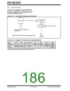
PIC18CXX2
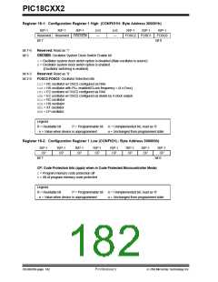
Register 18-1: Configuration Register 1 High (CONFIG1H: Byte Address 300001h)
R/P-1
R/P-1
R/P-1
U-0
U-0
R/P-1
R/P-1
R/P-1
FOSC0
bit 0
Reserved Reserved OSCSEN
—
—
FOSC2 FOSC1
bit 7
bit 7-6
bit 5
Reserved: Read as ’1’
OSCSEN: Oscillator System Clock Switch Enable bit
1= Oscillator system clock switch option is disabled (Main oscillator is source)
0= Oscillator system clock switch option is enabled
(Oscillator switching is enabled)
bit 4-3
bit 2-0
Reserved: Read as ’0’
FOSC2:FOSC0: Oscillator Selection bits
111= RC oscillator w/ OSC2 configured as RA6
110= HS oscillator with PLL enabled/CLock frequency = (4 x Fosc)
101= EC oscillator w/ OSC2 configured as RA6
100= EC oscillator w/ OSC2 configured as divide by 4 clock output
011= RC oscillator
010= HS oscillator
001= XT oscillator
000= LP oscillator
Legend:
R = Readable bit
P = Programmable bit U = Unimplemented bit, read as ‘0’
u = Unchanged from programmed state
- n = Value when device is unprogrammed
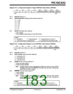
Register 18-2: Configuration Register 1 Low (CONFIG1L: Byte Address 300000h)
R/P-1
CP
R/P-1
CP
R/P-1
CP
R/P-1
CP
R/P-1
CP
R/P-1
CP
R/P-1
CP
R/P-1
CP
bit 7
bit 0
CP: Code Protection bits (apply when in Code Protected Microcontroller Mode)
1= Program memory code protection off
0= All of program memory code protected
Legend:
R = Readable bit
P = Programmable bit U = Unimplemented bit, read as ‘0’
- n = Value when device is unprogrammed
u = Unchanged from programmed state
DS39026B-page 182
Preliminary
7/99 Microchip Technology Inc.

 MICROCHIP [ MICROCHIP ]