PIC18CXX2
SLEEP mode is designed to offer a very low current
power-down mode. The user can wake-up from SLEEP
through external reset, Watchdog Timer Wake-up or
through an interrupt. Several oscillator options are also
made available to allow the part to fit the application.
The RC oscillator option saves system cost, while the
LP crystal option saves power. A set of configuration
bits are used to select various options.
18.0 SPECIAL FEATURES OF THE
CPU
There are several features intended to maximize sys-
tem reliability, minimize cost through elimination of
external components, provide power saving operating
modes and offer code protection. These are:
• OSC Selection
• Reset
18.1
Configuration Bits
- Power-on Reset (POR)
- Power-up Timer (PWRT)
- Oscillator Start-up Timer (OST)
- Brown-out Reset (BOR)
• Interrupts
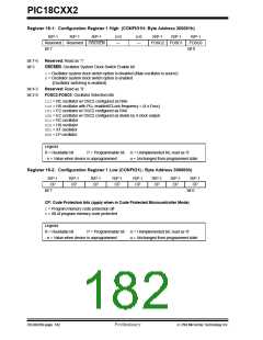
The configuration bits can be programmed (read as '0')
or left unprogrammed (read as '1') to select various
device configurations. These bits are mapped starting
at program memory location 300000h.
The user will note that address 300000h is beyond the
user program memory space. In fact, it belongs to the
configuration memory space (300000h - 3FFFFFh),
which can only be accessed using table reads and
table writes.
• Watchdog Timer (WDT)
• SLEEP
• Code protection
• ID locations
• In-circuit serial programming
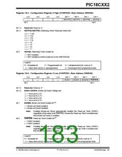
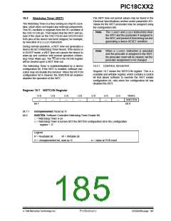
These devices have a Watchdog Timer, which is per-
manently enabled via the configuration bits or software-
controlled. It runs off its own RC oscillator for added
reliability. There are two timers that offer necessary
delays on power-up. One is the Oscillator Start-up
Timer (OST), intended to keep the chip in reset until the
crystal oscillator is stable. The other is the Power-up
Timer (PWRT), which provides a fixed delay on power-
up only, designed to keep the part in reset while the
power supply stabilizes. With these two timers on-chip,
most applications need no external reset circuitry.
TABLE 18-1: CONFIGURATION BITS AND DEVICE IDS
Default/
unprogrammed
value
Filename
Bit 7
Bit 6
Bit 5
Bit 4
Bit 3
Bit 2
Bit 1
Bit 0
300000h
300001h
300002h
300003h
300005h
300006h
3FFFFEh
3FFFFFh
CONFIG1L
CP
CP
CP
CP
CP
CP
CP
CP
1111 1111
111- -111
---- 1111
---- 1111
---- ---1
---- --11
0000 0000
0000 0010
CONFIG1H
CONFIG2L
CONFIG2H
CONFIG3H
CONFIG4L
DEVID1
—
—
OSCSEN
—
—
—
FOSC2
BORV0
WDTPS1
—
FOSC1
BODEN
WDTPS0
—
FOSC0
PWRTEN
WDTEN
CCP2MX
STVREN
REV0
—
—
—
BORV1
WDTPS2
—
—
—
—
—
—
—
—
—
—
—
—
—
—
—
LVEN
DEV2
DEV10
DEV1
DEV9
DEV0
DEV8
REV4
DEV7
REV3
DEV6
REV2
DEV5
REV1
DEV4
DEVID2
DEV3
Legend: x = unknown, u = unchanged, - = unimplemented, q = value depends on condition, grayed cells are unimplemented read as 0
7/99 Microchip Technology Inc.
Preliminary
DS39026B-page 181

 MICROCHIP [ MICROCHIP ]