PIC18CXX2
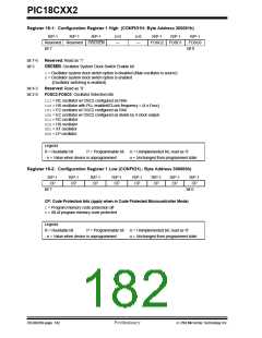
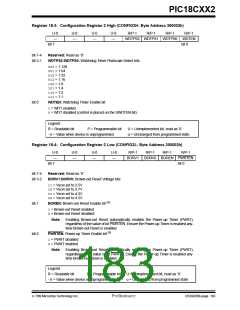
Register 18-3: Configuration Register 2 High (CONFIG2H: Byte Address 300003h)
U-0
U-0
U-0
U-0
R/P-1
R/P-1
R/P-1
R/P-1
—
—
—
—
WDTPS2 WDTPS1 WDTPS0 WDTEN
bit 0
bit 7
bit 7-4
bit 3-1
Reserved: Read as ’0’
WDTPS2:WDTPS0: Watchdog Timer Postscale Select bits
000= 1:128
001= 1:64
010= 1:32
011= 1:16
100= 1:8
101= 1:4
110= 1:2
111= 1:1
bit 0
WDTEN: Watchdog Timer Enable bit
1= WDT enabled
0= WDT disabled (control is placed on the SWDTEN bit)
Legend:
R = Readable bit
P = Programmable bit
U = Unimplemented bit, read as ‘0’
- n = Value when device is unprogrammed
u = Unchanged from programmed state
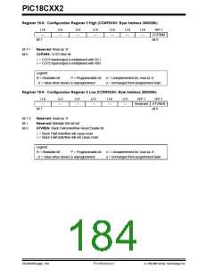
Register 18-4: Configuration Register 2 Low (CONFIG2L: Byte Address 300002h)
U-0
—
U-0
—
U-0
—
U-0
—
R/P-1
R/P-1
R/P-1
R/P-1
BORV1
BORV0 BOREN PWRTEN
bit 0
bit 7
bit 7-4
bit 3-2
Reserved: Read as ’0’
BORV1:BORV0: Brown-out Reset Voltage bits
11= VBOR set to 2.5V
10= VBOR set to 2.7V
01= VBOR set to 4.2V
00= VBOR set to 4.5V
bit 1
BOREN: Brown-out Reset Enable bit (1)
1= Brown-out Reset enabled
0= Brown-out Reset disabled
Note: Enabling Brown-out Reset automatically enables the Power-up Timer (PWRT),
regardless of the value of bit PWRTEN. Ensure the Power-up Timer is enabled any-
time Brown-out Reset is enabled.
bit 0
PWRTEN: Power-up Timer Enable bit (1)
1= PWRT disabled
0= PWRT enabled
Note: Enabling Brown-out Reset automatically enables the Power-up Timer (PWRT),
regardless of the value of bit PWRTE. Ensure the Power-up Timer is enabled any-
time Brown-out Reset is enabled.
Legend:
R = Readable bit
P = Programmable bit
U = Unimplemented bit, read as ‘0’
- n = Value when device is unprogrammed
u = Unchanged from programmed state
7/99 Microchip Technology Inc.
Preliminary
DS39026B-page 183

 MICROCHIP [ MICROCHIP ]