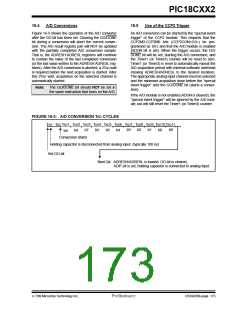
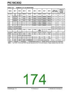
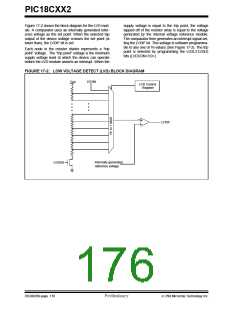
PIC18CXX2
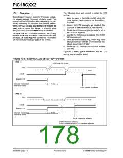
17.1
Control Register
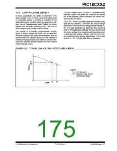
The Low Voltage Detect Control register controls the
operation of the Low Voltage Detect circuitry.
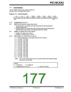
Register 17-1: LVDCON Register
U-0
U-0
R-0
R/W-0
R/W-0
R/W-1
R/W-0
LVDL1
R/W-1
—
—
IRVST
LVDEN
LVDL3
LVDL2
LVDL0
bit 7
bit 0
bit 7:6
bit 5
Unimplemented: Read as ’0’
IRVST: Internal Reference Voltage Stable Flag bit
1= Indicates that the Low Voltage Detect logic will generate the interrupt flag at the
specified voltage range.
0= Indicates that the Low Voltage Detect logic will not generate the interrupt flag at the
specified voltage range and the LVD interrupt should not be enabled
bit 4
LVDEN: Low-voltage Detect Power Enable bit
1= Enables LVD, powers up LVD circuit
0= Disables LVD, powers down LVD circuit
bit 3:0
LVDL3:LVDL0: Low Voltage Detection Limit bits
1111= External analog input is used (input comes from the LVDIN pin)
1110= 4.5V min - 4.77V max.
1101= 4.2V min - 4.45V max.
1100= 4.0V min - 4.24V max.
1011= 3.8V min - 4.03V max.
1010= 3.6V min - 3.82V max.
1001= 3.5V min - 3.71V max.
1000= 3.3V min - 3.50V max.
0111= 3.0V min - 3.18V max.
0110= 2.8V min - 2.97V max.
0101= 2.7V min - 2.86V max.
0100= 2.5V min - 2.65V max.
0011= 2.4V min - 2.54V max.
0010= 2.2V min - 2.33V max.
0001= 2.0V min - 2.12V max.
0000= 1.8V min - 1.91V max.
Note: LVDL3:LVDL0 modes which result in a trip point below the valid operating voltage
of the device are not tested.
Legend:
R = Readable bit
W = Writable bit
U = Unimplemented bit, read as ‘0’
- n = Value at POR reset
7/99 Microchip Technology Inc.
Preliminary
DS39026B-page 177

 MICROCHIP [ MICROCHIP ]