PIC18CXX2
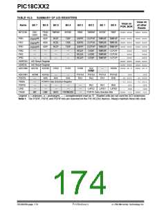
TABLE 16-3: SUMMARY OF A/D REGISTERS
Value on
all other
Resets
Value on
POR, BOR
Name
Bit 7
Bit 6
Bit 5
Bit 4
Bit 3
Bit 2
Bit 1
Bit 0
INTCON
GIE/
GIEH
PEIE/
GIEL
TMR0IE
INT0IE
RBIE
TMR0IF
INT0IF
RBIF
0000 000x
0000 000u
(1)
PIR1
PIE1
IPR1
ADIF
ADIE
ADIP
RCIF
RCIE
RCIP
TXIF
TXIE
TXIP
SSPIF
SSPIE
SSPIP
CCP1IF
CCP1IE
CCP1IP
TMR2IF TMR1IF 0000 0000
TMR2IE TMR1IE 0000 0000
TMR2IP TMR1IP 0000 0000
0000 0000
0000 0000
0000 0000
PSPIF
PSPIE
(1)
(1)
PSPIP
—
PIR2
—
—
—
—
—
—
—
—
—
BCLIF
BCLIE
BCLIP
LVDIF
LVDIE
LVDIP
TMR3IF
CCP2IF ---- 0000
---- 0000
---- 0000
---- 0000
uuuu uuuu
uuuu uuuu
0000 00-0
PIE2
—
TMR3IE CCP2IE ---- 0000
TMR3IP CCP2IP ---- 0000
xxxx xxxx
IPR2
—
ADRESH
ADRESL
ADCON0
A/D Result Register
A/D Result Register
xxxx xxxx
ADCS1
ADCS0
CHS2
CHS1
CHS0
GO/
—
ADON
0000 00-0
DONE
ADCON1
PORTA
TRISA
PORTE
LATE
ADFM
—
ADCS2
RA6
—
—
PCFG3
RA3
PCFG2
RA2
PCFG1
RA1
PCFG0 ---- -000
---- -000
--0u 0000
--11 1111
---- -000
---- -uuu
0000 -111
RA5
RA4
RA0
--0x 0000
--11 1111
---- -000
---- -xxx
0000 -111
—
PORTA Data Direction Register
—
—
—
—
—
—
—
—
—
—
RE2
RE1
RE0
—
LATE2
LATE1
LATE0
TRISE
IBF
OBF
IBOV
PSPMODE
PORTE Data Direction Bits
Legend: x = unknown, u = unchanged, — = unimplemented read as ’0’. Shaded cells are not used for A/D conversion.
Note 1: The PSPIF, PSPIE and PSPIP bits are reserved on the PIC18C2X2 devices. Always maintain these bits clear.
DS39026B-page 174
Preliminary
7/99 Microchip Technology Inc.

 MICROCHIP [ MICROCHIP ]