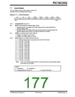
PIC18CXX2
16.4
A/D Conversions
16.5
Use of the CCP2 Trigger
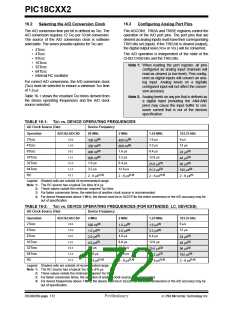
Figure 16-3 shows the operation of the A/D converter
after the GO bit has been set. Clearing the GO/DONE
bit during a conversion will abort the current conver-
sion. The A/D result register pair will NOT be updated
with the partially completed A/D conversion sample.
That is, the ADRESH:ADRESL registers will continue
to contain the value of the last completed conversion
(or the last value written to the ADRESH:ADRESL reg-
isters). After the A/D conversion is aborted, a 2TAD wait
is required before the next acquisition is started. After
this 2TAD wait, acquisition on the selected channel is
automatically started.
An A/D conversion can be started by the “special event
trigger” of the CCP2 module. This requires that the
CCP2M3:CCP2M0 bits (CCP2CON<3:0>) be pro-
grammed as 1011 and that the A/D module is enabled
(ADON bit is set). When the trigger occurs, the GO/
DONE bit will be set, starting the A/D conversion, and
the Timer1 (or Timer3) counter will be reset to zero.
Timer1 (or Timer3) is reset to automatically repeat the
A/D acquisition period with minimal software overhead
(moving ADRESH/ADRESL to the desired location).
The appropriate analog input channel must be selected
and the minimum acquisition done before the “special
event trigger” sets the GO/DONE bit (starts a conver-
sion).
Note: The GO/DONE bit should NOT be set in
the same instruction that turns on the A/D.
If the A/D module is not enabled (ADON is cleared), the
“special event trigger” will be ignored by the A/D mod-
ule, but will still reset the Timer1 (or Timer3) counter.
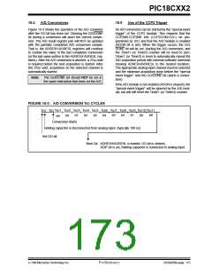
FIGURE 16-3: A/D CONVERSION TAD CYCLES
Tcy - TAD
TAD6 TAD7 TAD8 TAD9 TAD10 TAD11
TAD1 TAD2 TAD3 TAD4 TAD5
b7 b6
b5
b4
b3
b2
b1
b0
b0
b8
b9
Conversion Starts
Holding capacitor is disconnected from analog input (typically 100 ns)
Set GO bit
Next Q4: ADRESH/ADRESL is loaded, GO bit is cleared,
ADIF bit is set, holding capacitor is connected to analog input.
7/99 Microchip Technology Inc.
Preliminary
DS39026B-page 173

 MICROCHIP [ MICROCHIP ]