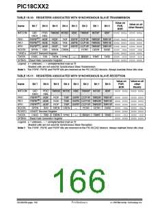
PIC18CXX2
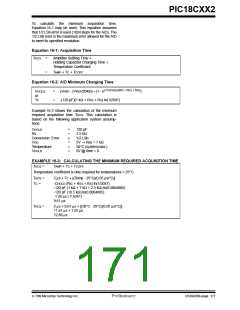
The value that is in the ADRESH/ADRESL registers is
not modified for a Power-on Reset. The ADRESH/
ADRESL registers will contain unknown data after a
Power-on Reset.
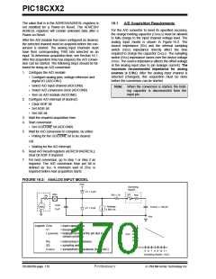
16.1
A/D Acquisition Requirements
For the A/D converter to meet its specified accuracy,
the charge holding capacitor (CHOLD) must be allowed
to fully charge to the input channel voltage level. The
analog input model is shown in Figure 16-2. The
source impedance (RS) and the internal sampling
switch (RSS) impedance directly affect the time
required to charge the capacitor CHOLD. The sampling
switch (RSS) impedance varies over the device voltage
(VDD). The source impedance affects the offset voltage
at the analog input (due to pin leakage current). The
maximum recommended impedance for analog
sources is 2.5kΩ. After the analog input channel is
selected (changed), this acquisition must be done
before the conversion can be started.
After the A/D module has been configured as desired,
the selected channel must be acquired before the con-
version is started. The analog input channels must
have their corresponding TRIS bits selected as an
input. To determine acquisition time, see Section 16.1.
After this acquisition time has elapsed, the A/D conver-
sion can be started. The following steps should be fol-
lowed for doing an A/D conversion:
1. Configure the A/D module:
• Configure analog pins, voltage reference and
digital I/O (ADCON1)
• Select A/D input channel (ADCON0)
• Select A/D conversion clock (ADCON0)
• Turn on A/D module (ADCON0)
2. Configure A/D interrupt (if desired):
• Clear ADIF bit
Note: When the conversion is started, the hold-
ing capacitor is disconnected from the
input pin.
• Set ADIE bit
• Set GIE bit
3. Wait the required acquisition time.
4. Start conversion:
• Set GO/DONE bit (ADCON0)
5. Wait for A/D conversion to complete, by either:
• Polling for the GO/DONE bit to be cleared
OR
• Waiting for the A/D interrupt
6. Read A/D Result registers (ADRESH/ADRESL);
clear bit ADIF if required.
7. For next conversion, go to step 1 or step 2 as
required. The A/D conversion time per bit is
defined as TAD. A minimum wait of 2TAD is
required before next acquisition starts.
FIGURE 16-2: ANALOG INPUT MODEL
VDD
Sampling
Switch
VT = 0.6V
ANx
Rs
SS
RIC ≤ 1k
RSS
CPIN
VAIN
I leakage
± 500 nA
CHOLD = 120 pF
VT = 0.6V
5 pF
VSS
Legend: CPIN
VT
= input capacitance
= threshold voltage
6V
5V
VDD 4V
I LEAKAGE = leakage current at the pin due to
various junctions
3V
2V
RIC
= interconnect resistance
= sampling switch
SS
CHOLD
= sample/hold capacitance (from DAC)
5
6 7 8 9 10 11
Sampling Switch ( kΩ )
DS39026B-page 170
Preliminary
7/99 Microchip Technology Inc.

 MICROCHIP [ MICROCHIP ]