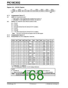
PIC18CXX2
16.2
Selecting the A/D Conversion Clock
16.3
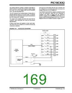
Configuring Analog Port Pins
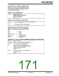
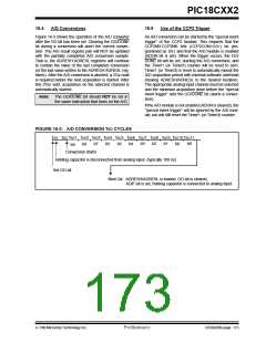
The A/D conversion time per bit is defined as TAD. The
A/D conversion requires 12 TAD per 10-bit conversion.
The source of the A/D conversion clock is software
selectable. The seven possible options for TAD are:
The ADCON1, TRISA and TRISE registers control the
operation of the A/D port pins. The port pins that are
desired as analog inputs must have their corresponding
TRIS bits set (input). If the TRIS bit is cleared (output),
the digital output level (VOH or VOL) will be converted.
• 2TOSC
• 4TOSC
• 8TOSC
The A/D operation is independent of the state of the
CHS2:CHS0 bits and the TRIS bits.
• 16TOSC
• 32TOSC
• 64TOSC
• Internal RC oscillator
Note 1: When reading the port register, all pins
configured as analog input channels will
read as cleared (a low level). Pins config-
ured as digital inputs will convert an ana-
log input. Analog levels on a digitally
configured input will not affect the conver-
sion accuracy.
For correct A/D conversions, the A/D conversion clock
(TAD) must be selected to ensure a minimum TAD time
of 1.6 µs.
Table 16-1 shows the resultant TAD times derived from
the device operating frequencies and the A/D clock
source selected.
Note 2: Analog levels on any pin that is defined as
a digital input (including the AN4:AN0
pins) may cause the input buffer to con-
sume current that is out of the devices
specification.
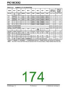
TABLE 16-1: TAD vs. DEVICE OPERATING FREQUENCIES
AD Clock Source (TAD)
Device Frequency
Operation
2TOSC
ADCS2:ADCS0
20 MHz
5 MHz
1.25 MHz
1.6 µs
333.33 kHz
6 µs
(2)
(2)
(2)
000
100
001
101
010
110
011
100 ns
400 ns
(2)
4TOSC
3.2 µs
12 µs
200 ns
800 ns
(2)
(3)
8TOSC
1.6 µs
6.4 µs
400 ns
24 µs
(2)
(3)
16TOSC
32TOSC
64TOSC
RC
3.2 µs
6.4 µs
12.8 µs
800 ns
48 µs
(3)
(3)
1.6 µs
3.2 µs
25.6 µs
96 µs
(3)
(3)
12.8 µs
2 - 6 µs
51.2 µs
192 µs
(1,4)
(1,4)
(1,4)
(1)
2 - 6 µs
2 - 6 µs
2 - 6 µs
Legend: Shaded cells are outside of recommended range.
Note 1: The RC source has a typical TAD time of 4 µs.
2: These values violate the minimum required TAD time.
3: For faster conversion times, the selection of another clock source is recommended.
4: For device frequencies above 1 MHz, the device must be in SLEEP for the entire conversion or the A/D accuracy may be
out of specification.
TABLE 16-2: TAD vs. DEVICE OPERATING FREQUENCIES (FOR EXTENDED, LC, DEVICES)
AD Clock Source (TAD)
Device Frequency
Operation
2TOSC
ADCS2:ADCS0
4 MHz
2 MHz
1.25 MHz
333.33 kHz
6 µs
(2)
(2)
(2)
000
100
001
101
010
110
011
500 ns
1.0 µs
1.6 µs
(2)
(2)
(2)
4TOSC
12 µs
1.0 µs
2.0 µs
4.0 µs
3.2 µs
(2)
(3)
8TOSC
6.4 µs
2.0 µs
24 µs
(2)
(3)
16TOSC
32TOSC
64TOSC
RC
8.0 µs
12.8 µs
4.0 µs
48 µs
(3)
(3)
8.0 µs
16.0 µs
32.0 µs
25.6 µs
96 µs
(3)
(3)
16.0 µs
51.2 µs
192 µs
(1,4)
(1,4)
(1,4)
(1,4)
3 - 9 µs
3 - 9 µs
3 - 9 µs
3 - 9 µs
Legend: Shaded cells are outside of recommended range.
Note 1: The RC source has a typical TAD time of 6 µs.
2: These values violate the minimum required TAD time.
3: For faster conversion times, the selection of another clock source is recommended.
4: For device frequencies above 1 MHz, the device must be in SLEEP for the entire conversion or the A/D accuracy may be
out of specification.
DS39026B-page 172
Preliminary
7/99 Microchip Technology Inc.

 MICROCHIP [ MICROCHIP ]