PIC18CXX2
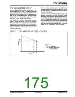
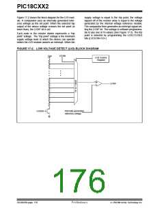
Figure 17-2 shows the block diagram for the LVD mod-
ule. A comparator uses an internally generated refer-
ence voltage as the set point. When the selected tap
output of the device voltage crosses the set point (is
lower than), the LVDIF bit is set.
supply voltage is equal to the trip point, the voltage
tapped off of the resistor array is equal to the voltage
generated by the internal voltage reference module.
The comparator then generates an interrupt signal set-
ting the LVDIF bit. This voltage is software programma-
ble to any one of 16 values (See Figure 17-2). The trip
point is selected by programming the LVDL3:LVDL0
bits (LVDCON<3:0>).
Each node in the resister divider represents a “trip
point” voltage. The “trip point” voltage is the minimum
supply voltage level at which the device can operate
before the LVD module asserts an interrupt. When the
FIGURE 17-2: LOW VOLTAGE DETECT (LVD) BLOCK DIAGRAM
VDD
LVDIN
LVD Control
Register
LVDIF
Internally generated
reference voltage
LVDEN
DS39026B-page 176
Preliminary
7/99 Microchip Technology Inc.

 MICROCHIP [ MICROCHIP ]