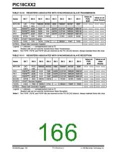
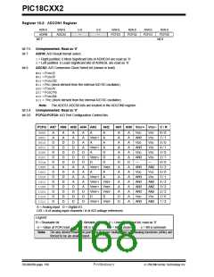
PIC18CXX2
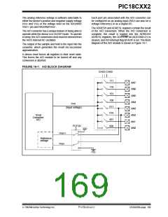
The analog reference voltage is software selectable to
either the device’s positive and negative supply voltage
(VDD and VSS) or the voltage level on the RA3/AN3/
VREF+ pin and RA2/AN2/VREF-.
Each port pin associated with the A/D converter can
be configured as an analog input (RA3 can also be a
voltage reference) or as a digital I/O.
The ADRESH and ADRESL registers contain the result
of the A/D conversion. When the A/D conversion is
complete, the result is loaded into the ADRESH/
ADRESL registers, the GO/DONE bit (ADCON0<2>) is
cleared, and A/D interrupt flag bit ADIF is set. The block
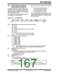
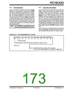
diagram of the A/D module is shown in Figure 16-1.
The A/D converter has a unique feature of being able to
operate while the device is in SLEEP mode. To operate
in sleep, the A/D conversion clock must be derived from
the A/D’s internal RC oscillator.
The output of the sample and hold is the input into the
converter, which generates the result via successive
approximation.
A device reset forces all registers to their reset state.
This forces the A/D module to be turned off and any
conversion is aborted.
FIGURE 16-1: A/D BLOCK DIAGRAM
CHS2:CHS0
111
AN7
110
AN6
101
AN5
100
AN4
VAIN
011
(Input voltage)
AN3
010
AN2
10-bit
Converter
A/D
001
AN1
PCFG0
000
AN0
VDD
VREF+
Reference
voltage
VREF-
VSS
7/99 Microchip Technology Inc.
Preliminary
DS39026B-page 169

 MICROCHIP [ MICROCHIP ]