PIC18CXX2
The A/D module has four registers. These registers
are:
16.0 10-BIT ANALOG-TO-DIGITAL
CONVERTER (A/D) MODULE
The analog-to-digital (A/D) converter module has five
inputs for the PIC18C2x2 devices and eight for the
PIC18C4x2 devices. This module has the ADCON0
and ADCON1 register definitions that are compatible
with the mid-range A/D module.
• A/D Result High Register (ADRESH)
• A/D Result Low Register (ADRESL)
• A/D Control Register 0 (ADCON0)
• A/D Control Register 1 (ADCON1)
The ADCON0 register, shown in Register 16-1, con-
trols the operation of the A/D module. The ADCON1
register, shown in Register 16-2, configures the func-
tions of the port pins.
The A/D allows conversion of an analog input signal to
a corresponding 10-bit digital number.
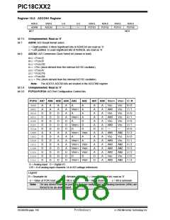
Register 16-1: ADCON0 Register
R/W-0
R/W-0
R/W-0
CHS2
R/W-0
CHS1
R/W-0
CHS0
R/W-0
U-0
R/W-0
ADCS1
ADCS0
GO/DONE
—
ADON
bit 7
bit 0
bit 7:6
ADCS1:ADCS0: A/D Conversion Clock Select bits (shown in bold)
000 = FOSC/2
001 = FOSC/8
010 = FOSC/32
011 = FRC (clock derived from the internal A/D RC oscillator)
100 = FOSC/4
101 = FOSC/16
110 = FOSC/64
111 = FRC (clock derived from the internal A/D RC oscillator)
Note: The ADCS2 bit is located in the ADCON1 register
CHS2:CHS0: Analog Channel Select bits
bit 5:3
000= channel 0, (AN0)
001= channel 1, (AN1)
010= channel 2, (AN2)
011= channel 3, (AN3)
100= channel 4, (AN4)
101= channel 5, (AN5)
110= channel 6, (AN6)
111= channel 7, (AN7)
Note: The PIC18C2X2 devices do not implement the full 8 A/D channels, the unimple-
mented selections are reserved. Do not select any unimplemented channel.
bit 2
GO/DONE: A/D Conversion Status bit
When ADON = 1
1= A/D conversion in progress (setting this bit starts the A/D conversion which is automatically
cleared by hardware when the A/D conversion is complete)
0= A/D conversion not in progress
Unimplemented: Read as ’0’
ADON: A/D On bit
bit 1
bit 0
1= A/D converter module is powered up
0= A/D converter module is shut off and consumes no operating current
Legend:
R = Readable bit
W = Writable bit
U = Unimplemented bit, read as ‘0’
’0’ = Bit is cleared x = Bit is unknown
- n = Value at POR reset
’1’ = Bit is set
7/99 Microchip Technology Inc.
Preliminary
DS39026B-page 167

 MICROCHIP [ MICROCHIP ]