PIC18CXX2
11.2
Timer2 Interrupt
11.3
Output of TMR2
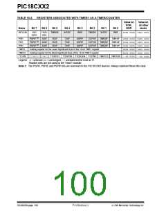
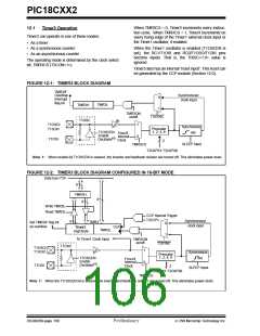
The Timer2 module has an 8-bit period register PR2.
Timer2 increments from 00h until it matches PR2 and
then resets to 00h on the next increment cycle. PR2 is
a readable and writable register. The PR2 register is ini-
tialized to FFh upon reset.
The output of TMR2 (before the postscaler) is fed to the
Synchronous Serial Port module, which optionally uses
it to generate the shift clock.
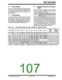
FIGURE 11-1: TIMER2 BLOCK DIAGRAM
Sets flag
TMR2
bit TMR2IF
output (1)
Prescaler
Reset
TMR2
FOSC/4
1:1, 1:4, 1:16
Postscaler
2
Comparator
1:1 to 1:16
EQ
T2CKPS1:T2CKPS0
4
PR2
TOUTPS3:TOUTPS0
Note 1: TMR2 register output can be software selected by the SSP Module as a baud clock.
TABLE 11-1: REGISTERS ASSOCIATED WITH TIMER2 AS A TIMER/COUNTER
Value on
all other
resets
Value on
POR, BOR
Name
Bit 7
Bit 6
Bit 5
Bit 4
Bit 3
Bit 2
Bit 1
Bit 0
INTCON
PIR1
GIE/GIEH PEIE/GIEL
TMR0IE
RCIF
INT0IE
TXIF
RBIE
SSPIF
SSPIE
SSPIP
TMR0IF
CCP1IF
CCP1IE
CCP1IP
INT0IF
TMR2IF
TMR2IE
TMR2IP
RBIF
0000 000x
0000 0000
0000 0000
0000 0000
0000 0000
-000 0000
1111 1111
0000 000u
0000 0000
0000 0000
0000 0000
0000 0000
-000 0000
1111 1111
PSPIF (1)
PSPIE (1)
PSPIP (1)
ADIF
ADIE
ADIP
TMR1IF
TMR1IE
TMR1IP
PIE1
RCIE
TXIE
TXIP
IPR1
RCIP
TMR2
T2CON
PR2
Timer2 module’s register
TOUTPS3
Timer2 Period Register
—
TOUTPS2
TOUTPS1
TOUTPS0
TMR2ON
T2CKPS1
T2CKPS0
Legend: x = unknown, u = unchanged, - = unimplemented read as ’0’. Shaded cells are not used by the Timer2 module.
Note 1: The PSPIF, PSPIE and PSPIP bits are reserved on the PIC18C2X2 devices. Always maintain these bits clear.
7/99 Microchip Technology Inc.
Preliminary
DS39026B-page 103

 MICROCHIP [ MICROCHIP ]