PIC18CXX2
11.1
Timer2 Operation
11.0 TIMER2 MODULE
The Timer2 module timer has the following features:
Timer2 can be used as the PWM time-base for the
PWM mode of the CCP module. The TMR2 register is
readable and writable, and is cleared on any device
reset. The input clock (FOSC/4) has a prescale option of
1:1, 1:4 or 1:16, selected by control bits
T2CKPS1:T2CKPS0 (T2CON<1:0>). The match out-
put of TMR2 goes through a 4-bit postscaler (which
gives a 1:1 to 1:16 scaling inclusive) to generate a
TMR2 interrupt (latched in flag bit TMR2IF, (PIR1<1>)).
• 8-bit timer (TMR2 register)
• 8-bit period register (PR2)
• Readable and writable (both registers)
• Software programmable prescaler (1:1, 1:4, 1:16)
• Software programmable postscaler (1:1 to 1:16)
• Interrupt on TMR2 match of PR2
• SSP module optional use of TMR2 output to gen-
erate clock shift
The prescaler and postscaler counters are cleared
when any of the following occurs:
Timer2 has a control register shown in Register 11-1.
Timer2 can be shut off by clearing control bit TMR2ON
(T2CON<2>) to minimize power consumption.
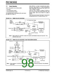
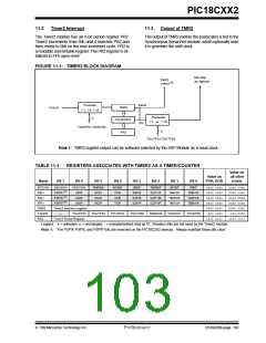
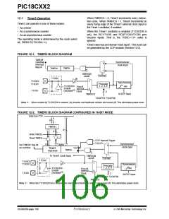
Figure 11-1 is a simplified block diagram of the Timer2
module. Figure 11-1 shows the Timer2 control register.
The prescaler and postscaler selection of Timer2 are
controlled by this register.
• a write to the TMR2 register
• a write to the T2CON register
• any device reset (Power-on Reset, MCLR reset,
Watchdog Timer reset, or Brown-out Reset)
TMR2 is not cleared when T2CON is written.
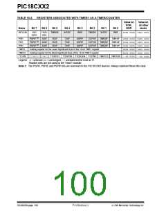
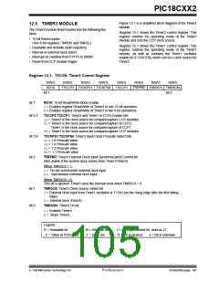
Register 11-1: T2CON: Timer2 Control Register
U-0
—
R/W-0
R/W-0
R/W-0
R/W-0
R/W-0
R/W-0
R/W-0
TOUTPS3 TOUTPS2 TOUTPS1 TOUTPS0 TMR2ON T2CKPS1 T2CKPS0
bit 0
bit
7
bit 7
Unimplemented: Read as '0'
bit 6:3
TOUTPS3:TOUTPS0: Timer2 Output Postscale Select bits
0000= 1:1 Postscale
0001= 1:2 Postscale
•
•
•
1111= 1:16 Postscale
bit 2
TMR2ON: Timer2 On bit
1= Timer2 is on
0= Timer2 is off
bit 1:0
T2CKPS1:T2CKPS0: Timer2 Clock Prescale Select bits
00= Prescaler is 1
01= Prescaler is 4
1x = Prescaler is 16
Legend:
R = Readable bit
W = Writable bit
’1’ = Bit is set
U = Unimplemented bit, read as ‘0’
’0’ = Bit is cleared x = Bit is unknown
- n = Value at POR reset
DS39026B-page 102
Preliminary
7/99 Microchip Technology Inc.

 MICROCHIP [ MICROCHIP ]