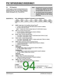
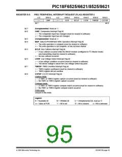
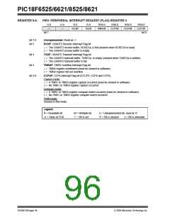
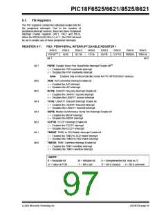
PIC18F6525/6621/8525/8621
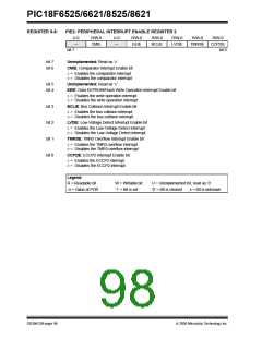
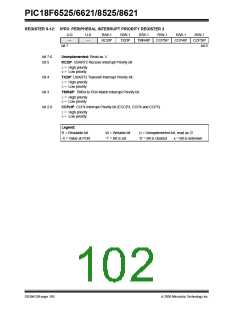
REGISTER 9-8:
PIE2: PERIPHERAL INTERRUPT ENABLE REGISTER 2
U-0
—
R/W-0
CMIE
U-0
—
R/W-0
EEIE
R/W-0
BCLIE
R/W-0
LVDIE
R/W-0
R/W-0
TMR3IE
CCP2IE
bit 7
bit 0
bit 7
bit 6
Unimplemented: Read as ‘0’
CMIE: Comparator Interrupt Enable bit
1= Enables the comparator interrupt
0= Disables the comparator interrupt
bit 5
bit 4
Unimplemented: Read as ‘0’
EEIE: Data EEPROM/Flash Write Operation Interrupt Enable bit
1= Enables the write operation interrupt
0= Disables the write operation interrupt
bit 3
bit 2
bit 1
bit 0
BCLIE: Bus Collision Interrupt Enable bit
1= Enables the bus collision interrupt
0= Disables the bus collision interrupt
LVDIE: Low-Voltage Detect Interrupt Enable bit
1= Enables the Low-Voltage Detect interrupt
0= Disables the Low-Voltage Detect interrupt
TMR3IE: TMR3 Overflow Interrupt Enable bit
1= Enables the TMR3 overflow interrupt
0= Disables the TMR3 overflow interrupt
CCP2IE: ECCP2 Interrupt Enable bit
1= Enables the ECCP2 interrupt
0= Disables the ECCP2 interrupt
Legend:
R = Readable bit
-n = Value at POR
W = Writable bit
‘1’ = Bit is set
U = Unimplemented bit, read as ‘0’
‘0’ = Bit is cleared x = Bit is unknown
DS39612B-page 96
2005 Microchip Technology Inc.

 MICROCHIP [ MICROCHIP ]