PIC18F6525/6621/8525/8621
17.1.3
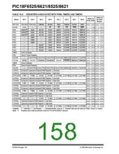
ECCP MODULES AND TIMER
RESOURCES
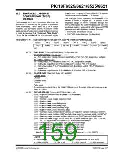
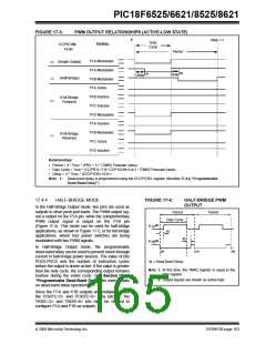
17.4 Enhanced PWM Mode
The Enhanced PWM mode provides additional PWM
output options for a broader range of control applica-
tions. The module is a backward compatible version of
the standard CCP module and offers up to four outputs,
designated PxA through PxD. Users are also able to
select the polarity of the signal (either active-high or
active-low). The module’s output mode and polarity
are configured by setting the PxM1:PxM0 and
CCPxM3CCPxM0 bits of the CCPxCON register
(CCPxCON<7:6> and CCPxCON<3:0>, respectively).
Like the standard CCP modules, the ECCP modules
can utilize Timers 1, 2, 3 or 4, depending on the mode
selected. Timer1 and Timer3 are available for modules
in Capture or Compare modes, while Timer2 and
Timer4 are available for modules in PWM mode.
Additional details on timer resources are provided in
Section 16.1.1
“CCP
Modules
and
Timer
Resources”.
17.2 Capture and Compare Modes
For the sake of clarity, Enhanced PWM mode operation
is described generically throughout this section with
respect to ECCP1 and TMR2 modules. Control register
names are presented in terms of ECCP1. All three
Enhanced modules, as well as the two timer resources,
can be used interchangeably and function identically.
TMR2 or TMR4 can be selected for PWM operation by
selecting the proper bits in T3CON.
Except for the operation of the special event trigger
discussed below, the Capture and Compare modes of
the ECCP module are identical in operation to that of
CCP4. These are discussed in detail in Section 16.2
“Capture Mode” and Section 16.3 “Compare
Mode”.
17.2.1
SPECIAL EVENT TRIGGER
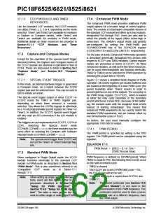
Figure 17-1 shows a simplified block diagram of PWM
operation. All control registers are double-buffered and
are loaded at the beginning of a new PWM cycle (the
period boundary when Timer2 resets) in order to
prevent glitches on any of the outputs. The exception is
the PWM Delay register, ECCP1DEL, which is loaded
at either the duty cycle boundary or the boundary
period (whichever comes first). Because of the buffer-
ing, the module waits until the assigned timer resets
instead of starting immediately. This means that
Enhanced PWM waveforms do not exactly match the
standard PWM waveforms, but are instead offset by
one full instruction cycle (4 TOSC).
In this mode, an internal hardware trigger is generated
in Compare mode, on a match between the CCPR
register pair and the selected timer. This can be used in
turn to initiate an action.
The special event trigger output of either ECCP1 or
ECCP2 resets the TMR1 or TMR3 register pair,
depending on which timer resource is currently
selected. This allows the CCPRx register to effectively
be a 16-bit programmable period register for Timer1 or
Timer3. In addition, the ECCP2 special event trigger
will also start an A/D conversion if the A/D module is
enabled.
As before, the user must manually configure the
appropriate TRIS bits for output.
The triggers are not implemented for ECCP3, CCP4 or
CCP5. Selecting the Special Event mode
(CCPxM3:CCPxM0 = 1011) for these modules has the
same effect as selecting the Compare with Software
Interrupt mode (CCPxM3:CCPxM0 = 1010).
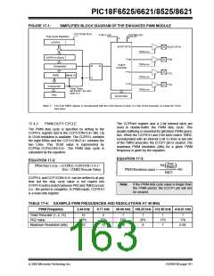
17.4.1
PWM PERIOD
The PWM period is specified by writing to the PR2
register. The PWM period can be calculated using the
equation:
Note:
The special event trigger from ECCP2 will
not set the Timer1 or Timer3 interrupt flag
bits.
EQUATION 17-1:
PWM Period = [(PR2) + 1] • 4 • TOSC •
(TMR2 Prescale Value)
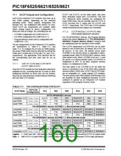
17.3 Standard PWM Mode
PWM frequency is defined as 1/[PWM period]. When
TMR2 is equal to PR2, the following three events occur
on the next increment cycle:
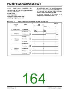
When configured in Single Output mode, the ECCP
module functions identically to the standard CCP
module in PWM mode as described in Section 16.4
“PWM Mode”. This is also sometimes referred to as
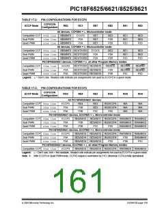
“Compatible CCP” mode as in Tables 17-1
through 17-3.
• TMR2 is cleared
• The ECCP1 pin is set (if PWM duty cycle = 0%,
the ECCP1 pin will not be set)
• The PWM duty cycle is copied from CCPR1L into
CCPR1H
Note:
When setting up single output PWM opera-
tions, users are free to use either of the
processes described in Section 16.4.3
“Setup for PWM Operation” or
Section 17.4.9 “Setup for PWM Opera-
tion”. The latter is more generic but will
work for either single or multi-output PWM.
Note:
The Timer2 postscaler (see Section 13.0
“Timer2 Module”) is not used in the
determination of the PWM frequency. The
postscaler could be used to have a servo
update rate at a different frequency than
the PWM output.
DS39612B-page 160
2005 Microchip Technology Inc.

 MICROCHIP [ MICROCHIP ]