PIC18F6525/6621/8525/8621
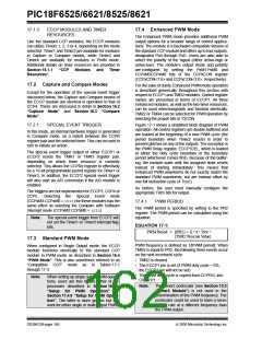
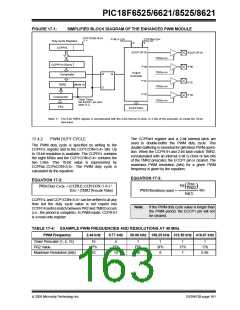
FIGURE 17-1:
SIMPLIFIED BLOCK DIAGRAM OF THE ENHANCED PWM MODULE
CCP1CON<5:4>
P1M1<1:0>
CCP1M<3:0>
4
Duty Cycle Registers
2
CCPR1L
ECCP1/P1A
P1B
ECCP1/P1A
P1B
TRISx<x>
TRISx<x>
TRISx<x>
TRISx<x>
CCPR1H (Slave)
Comparator
Output
Controller
R
S
Q
P1C
P1C
P1D
(Note 1)
TMR2
P1D
Comparator
PR2
Clear Timer,
set ECCP1 pin and
latch D.C.
ECCP1DEL
Note 1: The 8-bit TMR2 register is concatenated with the 2-bit internal Q clock, or 2 bits of the prescaler, to create the 10-bit
time base.
The CCPRxH register and a 2-bit internal latch are
used to double-buffer the PWM duty cycle. This
double-buffering is essential for glitchless PWM opera-
tion. When the CCPR1H and 2-bit latch match TMR2,
concatenated with an internal 2-bit Q clock or two bits
of the TMR2 prescaler, the ECCP1 pin is cleared. The
maximum PWM resolution (bits) for a given PWM
frequency is given by the equation:
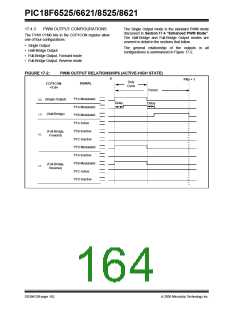
17.4.2
PWM DUTY CYCLE
The PWM duty cycle is specified by writing to the
CCPR1L register and to the CCP1CON<5:4> bits. Up
to 10-bit resolution is available. The CCPR1L contains
the eight MSbs and the CCP1CON<5:4> contains the
two LSbs. This 10-bit value is represented by
CCPRxL:CCPxCON<5:4>. The PWM duty cycle is
calculated by the equation:
EQUATION 17-3:
EQUATION 17-2:
FOSC
log
PWM Duty Cycle = (CCPR1L:CCP1CON<5:4>) •
TOSC • (TMR2 Prescale Value)
(FPWM)
bits
PWM Resolution (max) =
log(2)
CCPR1L and CCP1CON<5:4> can be written to at any
time but the duty cycle value is not copied into
CCPR1H until a match between PR2 and TMR2 occurs
(i.e., the period is complete). In PWM mode, CCPR1H
is a read-only register.
Note:
If the PWM duty cycle value is longer than
the PWM period, the ECCP1 pin will not
be cleared.
TABLE 17-4: EXAMPLE PWM FREQUENCIES AND RESOLUTIONS AT 40 MHz
PWM Frequency
2.44 kHz
9.77 kHz
39.06 kHz 156.25 kHz 312.50 kHz 416.67 kHz
Timer Prescaler (1, 4, 16)
PR2 Value
16
FFh
10
4
1
1
3Fh
8
1
1Fh
7
1
FFh
10
FFh
10
17h
6.58
Maximum Resolution (bits)
2005 Microchip Technology Inc.
DS39612B-page 161

 MICROCHIP [ MICROCHIP ]