PIC18F6525/6621/8525/8621
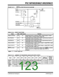
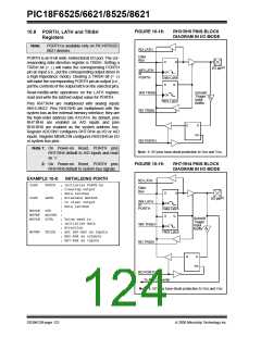
FIGURE 10-18:
RH3:RH0 PINS BLOCK
DIAGRAM IN I/O MODE
10.8 PORTH, LATH and TRISH
Registers
Note:
PORTH is available only on PIC18F8525/
8621 devices.
RD LATH
Data
Bus
PORTH is an 8-bit wide, bidirectional I/O port. The cor-
responding data direction register is TRISH. Setting a
TRISH bit (= 1) will make the corresponding PORTH
pin an input (i.e., put the corresponding output driver in
a high-impedance mode). Clearing a TRISH bit (= 0)
will make the corresponding PORTH pin an output (i.e.,
put the contents of the output latch on the selected pin).
D
Q
I/O pin(1)
WR LATH
or
PORTH
CK
Data Latch
D
Q
Read-modify-write operations on the LATH register,
read and write the latched output value for PORTH.
Schmitt
Trigger
Input
WR TRISH
RD TRISH
CK
TRIS Latch
Buffer
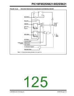
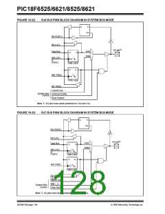
Pins RH7:RH4 are multiplexed with analog inputs
AN15:AN12. Pins RH3:RH0 are multiplexed with the
system bus as the external memory interface; they are
the high-order address bits A19:A16. By default, pins
RH7:RH4 are enabled as A/D inputs and pins
RH3:RH0 are enabled as the system address bus.
Register ADCON1 configures RH7:RH4 as I/O or A/D
inputs. Register MEMCON configures RH3:RH0 as I/O
or system bus pins.
Q
D
EN
EN
RD PORTH
Note 1: On Power-on Reset, PORTH pins
RH7:RH4 default to A/D inputs and read
as ‘0’.
Note 1: I/O pins have diode protection to VDD and VSS.
2: On Power-on Reset, PORTH pins
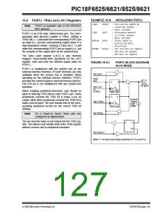
FIGURE 10-19:
RH7:RH4 PINS BLOCK
DIAGRAM IN I/O MODE
RH3:RH0 default to system bus signals.
EXAMPLE 10-8:
INITIALIZING PORTH
RD LATH
CLRF
PORTH
; Initialize PORTH by
; clearing output
; data latches
; Alternate method
; to clear output
; data latches
;
Data
Bus
D
Q
I/O pin(1)
CLRF
LATH
WR LATH
or
PORTH
CK
Data Latch
MOVLW
MOVWF
MOVLW
0Fh
ADCON1
0CFh
;
D
Q
Schmitt
Trigger
Input
; Value used to
; initialize data
; direction
WR TRISH
CK
TRIS Latch
Buffer
MOVWF
TRISH
; Set RH3:RH0 as inputs
; RH5:RH4 as outputs
; RH7:RH6 as inputs
RD TRISH
Q
D
EN
EN
RD PORTH
To A/D Converter
Note 1: I/O pins have diode protection to VDD and VSS.
DS39612B-page 122
2005 Microchip Technology Inc.

 MICROCHIP [ MICROCHIP ]