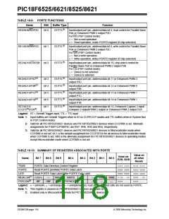
PIC18F6525/6621/8525/8621
The sixth pin of PORTG (MCLR/VPP/RG5) is a digital
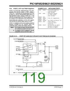
10.7 PORTG, TRISG and LATG
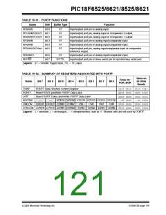
Registers
input pin. Its operation is controlled by the MCLRE
configuration bit in Configuration Register 3H
(CONFIG3H<7>). In its default configuration
(MCLRE = 1), the pin functions as the device Master
Clear input. When selected as a port pin (MCLRE = 0),
it functions as an input only pin; as such, it does not
have TRISG or LATG bits associated with it.
PORTG is a 6-bit wide port with 5 bidirectional pins
(RG0:RG4) and one optional input only pin (RG5). The
corresponding data direction register is TRISG. Setting
a TRISG bit (= 1) will make the corresponding PORTG
pin an input (i.e., put the corresponding output driver in
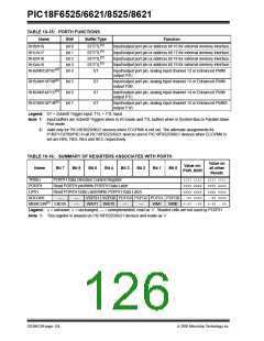
a high-impedance mode). Clearing a TRISG bit (= 0)
will make the corresponding PORTC pin an output (i.e.,
put the contents of the output latch on the selected pin).
In either configuration, RG5 also functions as the
programming voltage input during device programming.
Note 1: On a Power-on Reset, RG5 is enabled as
The Data Latch register (LATG) is also memory
mapped. Read-modify-write operations on the LATG
register, read and write the latched output value for
PORTG.
a
digital input only if Master Clear
functionality is disabled (MCLRE = 0).
2: If the device Master Clear is disabled,
verify that either of the following is done to
ensure proper entry into ICSP mode:
a.) disable low-voltage programming
(CONFIG4L<2> = 0); or
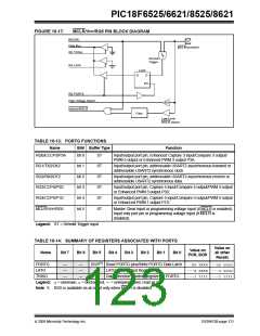
PORTG is multiplexed with both CCP/ECCP and
EUSART functions (Table 10-13). PORTG pins have
Schmitt Trigger input buffers.
When enabling peripheral functions, care should be
taken in defining TRIS bits for each PORTG pin. Some
peripherals override the TRIS bit to make a pin an
output, while other peripherals override the TRIS bit to
make a pin an input. The user should refer to the
corresponding peripheral section for the correct TRIS
bit settings.
b.) make certain that RB5/KBI1/PGM is
held low during entry into ICSP.
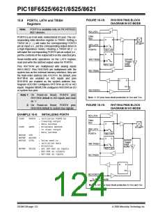
EXAMPLE 10-7:
INITIALIZING PORTG
CLRF
PORTG
; Initialize PORTG by
; clearing output
; data latches
CLRF
LATG
; Alternate method
; to clear output
; data latches
Note:
On a Power-on Reset, these pins are
configured as digital inputs.
The pin override value is not loaded into the TRIS reg-
ister. This allows read-modify-write operations of the
TRIS register without concern due to peripheral
overrides.
MOVLW
MOVWF
0x04
; Value used to
; initialize data
; direction
; Set RG1:RG0 as outputs
; RG2 as input
TRISG
; RG4:RG3 as inputs
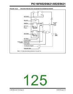
FIGURE 10-16:
PORTG BLOCK DIAGRAM (PERIPHERAL OUTPUT OVERRIDE)
TRIS OVERRIDE
PORTG/Peripheral Out Select
Peripheral Data Out
Pin
Override
Peripheral
VDD
P
0
1
RG0
RG1
Yes
Yes
ECCP3 I/O
USART1 Async Xmit,
Sync Clock
RD LATG
RG2
Yes
USART1 Async Rcv,
Sync Data Out
Data Bus
D
Q
Q
I/O pin(1)
WR LATG or
CK
RG3
RG4
Yes
Yes
CCP4 I/O
CCP5 I/O
WR PORTG
Data Latch
N
D
Q
Q
Note 1: I/O pins have diode protection to VDD
VSS
and VSS.
TRIS
Override
Logic
WR TRISG
CK
2: Peripheral output enable is only active
if peripheral select is active.
TRIS Latch
RD TRISG
Schmitt
Trigger
Peripheral Output
Enable(2)
Q
D
EN
RD PORTG
Peripheral Data In
DS39612B-page 120
2005 Microchip Technology Inc.

 MICROCHIP [ MICROCHIP ]