PIC18F6525/6621/8525/8621
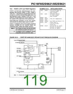
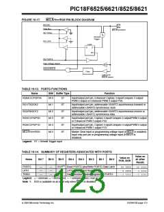
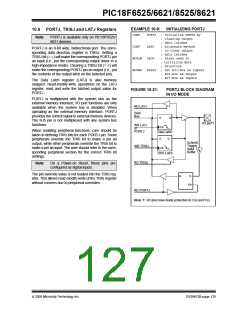
FIGURE 10-17:
MCLR/VPP/RG5 PIN BLOCK DIAGRAM
MCLRE
Data Bus
MCLR/VPP/RG5
RD TRISA
Schmitt
Trigger
RD LATA
Latch
Q
D
EN
RD PORTA
High-Voltage Detect
HV
Internal MCLR
Filter
Low-Level
MCLR Detect
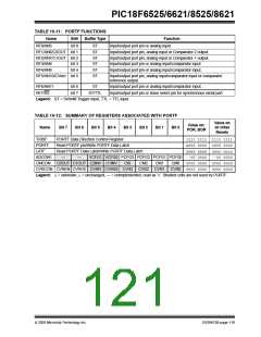
TABLE 10-13: PORTG FUNCTIONS
Name
Bit# Buffer Type
Function
RG0/ECCP3/P3A
bit 0
bit 1
bit 2
bit 3
bit 4
bit 5
ST
ST
ST
ST
ST
ST
Input/output port pin, Enhanced Capture 3 input/Compare 3 output/
PWM 3 output or Enhanced PWM 3 output P3A.
RG1/TX2/CK2
RG2/RX2/DT2
RG3/CCP4/P3D
RG4/CCP5/P1D
MCLR/VPP/RG5
Input/output port pin, addressable USART2 asynchronous transmit or
addressable USART2 synchronous clock.
Input/output port pin, addressable USART2 asynchronous receive or
addressable USART2 synchronous data.
Input/output port pin, Capture 4 input/Compare 4 output/PWM 4 output
or Enhanced PWM 3 output P3D.
Input/output port pin, Capture 5 input/Compare 5 output/PWM 5 output
or Enhanced PWM 1 output P1D.
Master Clear input or programming voltage input (if MCLR is enabled).
Input only port pin or programming voltage input (if MCLR is
disabled).
Legend: ST = Schmitt Trigger input
TABLE 10-14: SUMMARY OF REGISTERS ASSOCIATED WITH PORTG
Value on
all other
Resets
Value on
POR, BOR
Name
Bit 7
Bit 6
Bit 5
Bit 4
Bit 3
Bit 2
Bit 1
Bit 0
PORTG
LATG
—
—
—
—
—
—
RG5(1) Read PORTG pins/Write PORTG Data Latch --xx xxxx --uu uuuu
—
—
LATG Data Output Register
---x xxxx ---u uuuu
---1 1111 ---1 1111
TRISG
Data Direction Control Register for PORTG
Legend: x= unknown, u= unchanged, — = unimplemented, read as ‘0’
Note 1: RG5 is available as an input only when MCLR is disabled.
2005 Microchip Technology Inc.
DS39612B-page 121

 MICROCHIP [ MICROCHIP ]