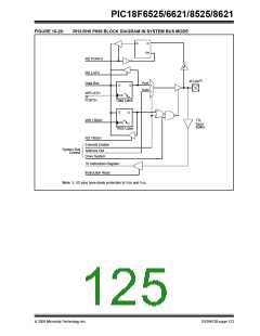
PIC18F6525/6621/8525/8621
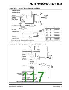
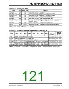
TABLE 10-11: PORTF FUNCTIONS
Name
RF0/AN5
Bit#
Buffer Type
Function
bit 0
ST
ST
ST
ST
ST
ST
Input/output port pin or analog input.
RF1/AN6/C2OUT bit 1
RF2/AN7/C1OUT bit 2
Input/output port pin, analog input or Comparator 2 output.
Input/output port pin, analog input or Comparator 1 output.
Input/output port pin or analog input/comparator input.
Input/output port pin or analog input/comparator input.
RF3/AN8
RF4/AN9
bit 3
bit 4
RF5/AN10/CVREF bit 5
Input/output port pin, analog input/comparator input or comparator
reference output.
RF6/AN11
RF7/SS
bit 6
bit 7
ST
Input/output port pin or analog input/comparator input.
ST/TTL
Input/output port pin or slave select pin for synchronous serial port.
Legend: ST = Schmitt Trigger input, TTL = TTL input
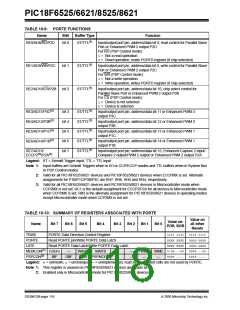
TABLE 10-12: SUMMARY OF REGISTERS ASSOCIATED WITH PORTF
Value on
all other
Resets
Value on:
POR, BOR
Name
Bit 7
Bit 6
Bit 5
Bit 4
Bit 3
Bit 2
Bit 1
Bit 0
TRISF
PORTF Data Direction Control Register
Read PORTF pin/Write PORTF Data Latch
Read PORTF Data Latch/Write PORTF Data Latch
1111 1111 1111 1111
x000 0000 u000 0000
xxxx xxxx uuuu uuuu
PORTF
LATF
ADCON1
CMCON
—
—
VCFG1 VCFG0 PCFG3 PCFG2 PCFG1 PCFG0 --00 0000 --00 0000
C2OUT C1OUT C2INV C1INV CIS CM2 CM1 CM0 0000 0000 0000 0000
CVRCON CVREN CVROE CVRR CVRSS CVR3 CVR2 CVR1 CVR0 0000 0000 0000 0000
Legend: x= unknown, u= unchanged, — = unimplemented, read as ‘0’. Shaded cells are not used by PORTF.
2005 Microchip Technology Inc.
DS39612B-page 119

 MICROCHIP [ MICROCHIP ]